WBo2 2D1 OEM Wideband Unit

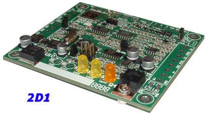
The 2D1 is Tech Edge's high quality SMD OEM wideband product for Bosch LSU (5 wire) sensors. It is an updated version of the through-hole 2D0 board that we still actively sell. 2D1 is slightly smaller than 2D0 and has the robustness of surface mount (SMD) construction. SMD is not so readily repaired but this isn't a problem as these units are very reliable and we repair most of our customer's devices anyway.

We designed 2D0/2D1 primarily for integration into other manufacturers' equipment as a basic wideband Lambda controller. but they are also suitable for other applications where our other units' in-built logging and other features are not required. 2D1 does have Auto-Cal, RPM & 3 analogue inputs and can log to a PC, but does not have on-board logging memory. 2D1 has the enhanced pump cell control technology found in all newer version 2.0 units.

The latest 2D1 PCB rev. can be ordered with analog 4-20 mA loop capability that is in addition to the 0-5 Volt WBlin 12 bit output. More info on the 2D1L below.

Since March 2011 we offer a finished version of this controller board. The 2DP Professional model comes in a diecast metal case and comes standard with 4-20mA loop capability.

We can, and have, customised the basic 2D1 design for specific OEM applications, interfaces and environments. Contact us for more information.

Tech Edge  2D1 Features

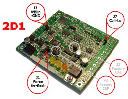
Move your mouse over the image above right to see some of 2D1's features. As you can see it's fairly small (here's an enlarged & annotated image or see 2D1 in plan view). PCB dimensions are 85 x 75 mm and around 12 mm high (allow 15 mm as highest points are the pin headers), and holes are on 65 mm & 75 mm centres (ie. 5 mm from board edges). If you want to integrate this board onto your own PCB then you'll need this engineering layout of mounting holes, etc. (PDF).

Other features include:


Buy the 2D1 Configured as Follows ...

unit with sensor, cable, and display & .

2D1 Display LSU Sensor Cable Other


Total price of selected item(s) : quantity : ...


Connection Overview for 2D1

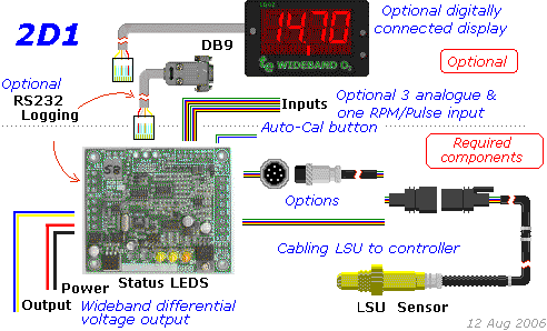
The image at right shows how 2D1 is connected to other WBo2 wideband components. Carefully note that the minimum connection requirements for a usable system are shown in the lower half of the diagram :

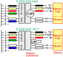
  • Seven sensor wires comprising four signal wires (Vs, Ip, Vs/Ip, Rcal) & a shield &, two heater wires (H+ & H-).
  • two wires for power (+12V & GND), and
  • two wires for wideband output (WBlin+ & WBlin+).
  • two wires for Auto-Cal press button (optional but strongly recommended).

There are a number of options for connecting the sensor to the controller including using a standard Tech Edge cable and standard 8 pin panel mount circular connector, then OEM cabling from the circular connector to the wideband unit itself. We recommend that the 4 signal wires to/from the sensor are shielded as this will improve noise immunity.

2D1 Inputs & Outputs - Details

The 2D1 Wideband unit, in its basic form, comes as a pre-built and tested PCB without any connectors mounted and without any sensor cabling - these can be provided or, as OEM manufacturer, you supply to your own specifications. 2D1 has the facility for 3 connectors of 5.08 mm (0.2") pitch, two of 2.54 mm (0.1") pitch, and a single RJ45 connector. The connectors are described below : Pin functions are listed in blue, the markings found on the PCB are shown in (italic red). Click on the schematic to see a pop-up image of the PCB area for the connector.

2D1 Purchase Options

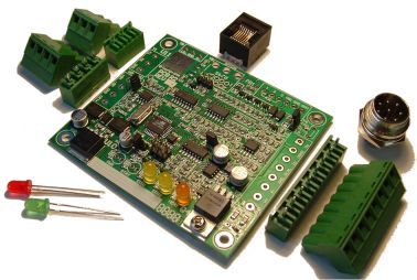
2D1 was designed to be a low cost unit (but quality has not been compromised) that's easily integrated into other devices. The 2D1 module can be supplied with or without connectors and these connectors can be mounted one of two ways. The additional connectors Tech Edge can supply include the three 5.08 mm (0.2") pitch headers (x3, x4 & x8) with their mating plug-in and screw-to connectors, RJ45, green power and red status LED, & circular 8 pin panel-mount cable connector. These are shown at left in front of the basic 2D1 unit. Click on the image for enlargement.

Note that the 0.2" (green) connectors shown will normally be supplied not soldered in as it's possible to insert them so the header leads face inwards (minimises the unit's footprint), or outwards (easy maintenance) and of course the pin numbering is then reversed.

The circular male 8 pin connector is the same as that found on other version 2.0 WBo2 units and is, solder bucket style & panel mount with the nut and washer behind the panel. This connector mates to a female 8 pin that is on the WBo2 end of the sensor cable. These cables are available in a few standard lengths (2.6 m & 4.0 m are the most popular).

An additional RS232 cable (with RJ45 and DB9 connector) for PC communications is available separately.

Jumper Shunts J1, J2, J3

Jumper shunts J1 & J2 are located at the centre of the board, J3 is located between pins 3 and 4 of the 0.2" headers. Click the image at left to enlarge.

J1 - (Rescue Re-flash) should normally be OFF (boards are supplied with the shunt sitting on one pin ONLY). To update the boards firmware the WButil.exe program is used in normal re-flash mode. Sometimes the 2D1's firmware can become corrupted and a special reflash operation using the J1 jumper is required.

J2 - (Factory-CAL) should normally be ON at all times, and is used for factory calibration and testing Note that free-air sensor calibration is quite different and is done using the WButil.exe utility or via the CAL button described below.

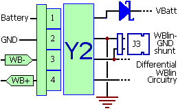
J3 - (WBlin-GND) provides a link between the SIG- (also called WBlin- on other units) output and GND and is used when a single ended output is required. Remove J3 when differential output is required, but in this case ensure WBlin- on the SIG- pin is connected to the destination input's GND_d point. For differential output there should not be more than a Volt of so difference GND_d and the 2D0's GND point. This topic is discussed further here.


WBlin+ Pin 4/Y2 & WBlin- Pin 3/Y2 Wideband Output
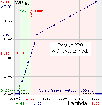
The WBlin output on 2D0 has default values a little different to other WBo2 units. Remember that the WBo2 configuration program WButil.exe lets you change these defaults.

Dual Slope Linear Output

Rather than the default linear AFR = 9.0 to 19.0 span of WBo2's standard 0 to 5 Volt output (see it here), 2D0 has a Lambda=0.65 to 3.0 span (*) over the 0.25 to 5.0 Volt range in two linear segments centered about Lambda = 1.2 at 3.25 Volts. This is shown in the graph at right. (* equivalent AFR range is 9.56 to 44.1). The effect of this is to reduce the resolution of the rich tuning range (AFR=9.6 to 17.6 covers 3.0 Volts) at the expense of better resolution in the lean range.

The actual formula for the dual slope follows the general straight line formula y=mx+c. In the formula below, L is Lambda, and V is voltage:

  • Rich (L = 0.65 -> 1.2) :   L = (0.55/3.0)*V + 0.60467    (ie. L = 0.18333*V + 0.60467)
  • Lean (L = 1.2 -> 3.0) :   L = (1.8/2.0)*V - 1.5                (ie. L = 0.9*V - 1.5)

Note very carefully, the rich graph starts at Lambda = 0.65 and a voltage of 0.25 Volts. The lean graph ends at a Lambda of 3.0 and Voltage of 5.0. Outside that range you should consult the next paragraph on Bounded Output. Lastly, note that stoich (ie. Lambda = 1.0) has a voltage of 2.159 Volts. To convert the above formulas to AFR, remember that:

  • AFR = AFRstoich * Lambda.

Bounded Output

Another 2D0 feature is the setting of valid Lambda limits by clamping WBlin to a fixed voltage when Lambda is higher or lower than the bounding limits. This scheme allows a recording device to determine if the WB output is valid (must be greater than 100 mV). The default Lambda bound limits are 0.65 and 3.0 and a bounding Voltage of 100 mV. If Lambda is richer or leaner than these values then WBlin will be fixed at 100 mV. In the image at right this is shown as the grey area to either side of the light green (rich) and the pink (lean) range. The actual clamped value is shown down the bottom in the light blue region.

It's possible to change the clamp values for 2D0 by modifying configuration parameters. The WButil.exe program is run, and in the Comms tab the following commands are manually entered in the Command box. The same program can re-program the output table(s) from the AFR Tables tab. This sequence defeats the clamping action by setting the rich Ipx threshold limit to 0 and the lean limit to 0x3000.

  • s6300   set low threshold (low) at 63 to 00 (hex value = rich Ipx threshold)
  • s6400   set low threshold (high) at 64 to 00
  • s6700   set high threshold (low) at 67 to 00
  • s6830   set high threshold (high) at 68 to 30 (lean Ipx threshold)
  • w         write to update the EEPROM (takes a seconds or so)

Remember that if you reflash the WBo2 unit with newer firmware, the setting entered above will be lost.

To automate the conversion of the standard 2D's dual slope settings to the 9-19 AFR settings over 0-5 Volts (ie. that is found on other WBo2 units as standard), use the 2D_0-5V_9-19AFR.zip and then use WButil to send it to the controller.


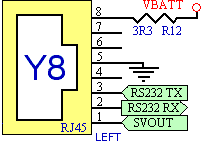
SVout Pin 1/Y8 (on RJ45) Compatibility Output

The SVout signal is intended for analogue displays like the LD01 but can be used as an alternate, lower resolution, single ended output.

To generate SVout, the processor uses a 65 word lookup table with linear interpolation. It converts the normalised pump current (Ipx) into a 10 bit value representing SVout. A hardware PWM (Pulse Width Modulation) pin on the processor generates the actual SVout voltage.

SVout is compatible with the Vout signal from the original oz-diy-wb unit (and the 1.5 unit's Vwb). It can be used to drive the analogue LD01 display (or the older 5301 if you change its connector).

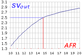
The default SVout, shown at right, varies between about 1.0 Volt for a very rich mixture (Lambda=0.6 or AFR=9), to 2.50 Volts for a stoic mixture, and to 3.1 Volts for a lean mixture (AFR=25). In free-air the SVout should be exactly 4.00 Volts when the unit has been free-air calibrated correctly.

The default AFR vs. SVout relationship is shown in the Vout table/graph page. The analogue Vout is a continuously available signal that may be logged with a high speed logger. We recommend at least a 10 bit converter for best accuracy, but as the measuring range is small (less than 3 Volts), measuring resolution is reduced compared to using a smaller AFR range over a larger voltage range.

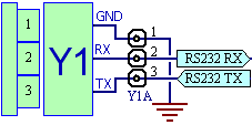
Serial RS232 Rx Pin 2/Y1, Tx Pin 3/Y1 & GND Pin 1/Y1

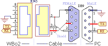
Note that as well as the three RS232 signals on Y1, for convenience, the RJ45 connector (Y8) also carries those same signals. click on the image to see the way the RJ45 is numbered. The 2D0 unit transmits logged data (Lambda/AFR and the analogue and pulse inputs) on its Tx line [pin 3] and receives commands (from PC or display) and code updates from a PC on its Rx line [pin 2].

The diagram at left shows the wires within the cable and also the connections at each end. Note the pin names change from left to right - the 2D0 unit's Tx pin transmits to the PC's Rx pin (and vice versa). [pin 1] is the shield for the Rx and Tx data lines as well as being the return data path.

WBo2 to PC cable

Here's an image of the actual RS232 cable for connection between a PC and 2D0's RJ45 connector. The cable is used for either logging to a PC, or for re-flashing its code (under control of a PC). If you need to extend the cable then a standard straight through male-female DB9 extension cable should be used (ie. not a cross-over or null modem cable).

RJ45 to DB9 cable

Serial Data logging - Lambda, Analogue & Pulse

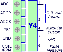
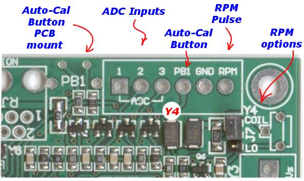
As noted above, as well as the Lambda/AFR data the unit collects, there are 3 unbuffered analogue inputs and a single pulse (can be used for RPM) input that can be logged.

The logged data is collected into an RS232 data frame that is fully described in the logging information section (default frame type is 1). The pins of the PCB for the inputs are shown in the diagram at right. This pop-up schematic of the inputs shows the unbuffered analogue inputs and the conditioned RPM/COIL input (here is the same schematic as a link.

As noted in the next section, the PB1 connection point parallels the on-board PB1 button (just to the left of the Y4 connector), and is for the Auto-Cal function.

Inbuilt Auto-Calibrate Function

The Auto-Calibrate feature eliminates the need for a PC to be used to calibrate the controller to a new sensor. A simple button press is used to start this free-air calibration process. Firstly ensure the sensor is sitting in perfectly clean air each time a calibration is performed. There is more information here on LSU sensor positioning that should also be consulted. If air at other than 20.9% oxygen content (ie. free-air) is used, or if large amounts of gaseous hydrocarbon are also preset, then the unit will NOT be correctly calibrated after the Auto-Cal operation.

Software : Firmware version 0658 or higher is required. Go to the HXF files page to download the latest files. The v command can be used to determine the firmware revision. The re-flash utility will automatically show the firmware version.

Hardware : A button and other parts must be added to the PCB (see Y4 described above). Note that the newer 2D1 model already includes the debounce and anti-static parts.

Operation : Press the Auto-Cal button for at least 1.5 seconds and no more than 4 (this is to avoid false triggering and also continuous operation with a stuck button - count 0, 1, 2 while holding the button). The red LED will begin fast flashing at about 4 flashes/second. If the sensor is in stable free-air then after After 15-20 seconds the LED will do three slower flashes indicating completion of the operation. At this point the free-air calibration value has been calculated and saved. You must perform the AutoCal operation again if it did not succeed, or it was performed inadvertently. The animated image at above right shows this - it takes almost 20 seconds to complete!

Advanced users should note that the Ipx-scaling value, being the result of the AutoCal operation, resides at config memory address 0x3B (low byte) and 0x3C (high byte). The g3b and the g3c commands display these two bytes.

Bosch LSU 4.9 support (PCB-R3 Aug. 2009)

The LSU 4.9 sensor is a newer sensor that may have benefits in some situations. It has slightly different characteristics to the LSU 4.0 and LSU 4.2 sensors and new firmware (downloadable here) is required due to higher internal operating impedance. Extended operation into the rich region (Lambda = 0.60) and more stable lean operation is claimed by Bosch. Prices of the LSU 4.9 sensors may drop as it becomes mainstream (Aug. '09).

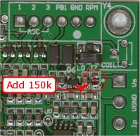
The latest rev of the 2D1 PCB (Rev 3) has a place for the 150k resistor described below. The image at left shows this 0805 sized SMD resistor just behind the 8 pin connector. Here is a larger pop-up image showing its location.

This resistor supplies the necessary bias current. It runs between Vs and +5 Volts. It must be removed if you revert to an LSU 4.0/4.2 (other models have a shunt, and a future 2D1 version will too!). Remember that you also need different firmware for the LSU 4.9 sensor that operates the heater at a different impedance and has other specific firmware modifications for PID operation, etc. The firmware is available from the HXF files section.

WARNING : Operating the LSU 4.9 with LSU 4.2 firmware will result in the heater being over driven and short sensor life or even sensor destruction. Using the LSU 4.2 with 4.9 firmware will also result in inaccurate results but, importantly, too-low heater temperature which may also shorten its life as it cannot burn off impurities.

Bosch LSU 4.9 support (PCB-R2 Apr. 2008)

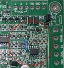
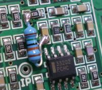
The image at left shows the 150k Ohm resistor that should be added to the component side of the 2D1 rev-2 board to add support for the LSU 4.9 sensor. The image at right shows the detail of the through hole resistor's soldering points on the PCB. Click on either image to enlarge.

WARNING : Operating the LSU 4.9 with LSU 4.2 firmware will result in the heater being over driven and short sensor life or even sensor destruction. Using the LSU 4.2 with 4.9 firmware will also result in inaccurate results but, importantly, too-low heater temperature which may also shorten its life as it cannot burn off impurities.

Analog 4-20 mA Current Loop Output (2D1L model)

The 2D1 can be ordered (from August 2009) with an additional analog 4-20 mA output option. This model is called the 2D1L. The additional 5 Volt regulator option described below cannot be ordered with this option as the same area of the PCB is used for both options.

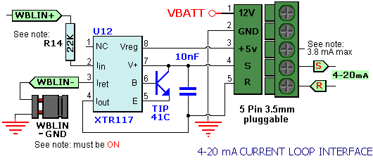
The schematic at right shows how the additional 4-20 mA circuit is connected to the WBlin Voltage output. The WBlin output can still be used but the voltage levels are programmed to correspond to the 4-20 mA loop values required. The circuit uses the industry standard XTR117 device from TI. Click on the image or here for a PCB layout diagram showing in particular where R14 is located.

Some very important points to note:

  • The 2D1L board cannot be powered from the loop current (the LSU sensor starting current of 3 Amps is almost 1,000 times this current!).
  • The [S] = Send and [R] = Receive pins on the 3.5 mm pluggable header are the 4-20 mA loop's Send (more positive) and Receive pins.
  • The loop receiver (in the remote equipment) must be electrically isolated from the 2D1L controller. In particular it must not share a common GROUND with the 2D1L.
  • R14 converts the 0-5 Volt signal to a current that is ultimately converted to the 4-20 mA loop current. WBlin is related to loop current as:
            I4-20 mA loop = 100 * WBlin/R14
    R14 is shipped as a 22kΩ resistor giving a loop current of 4 mA at 0.88 Volts, and 20 mA at 4.40 Volts. These two values should be used as the minimum and maximum WBlin values when reprogramming the WBlin output (using WButil). Refer to the board layout to locate R14 (to the immediate right of the TIP21C TO220 transistor).
  • For correct operation the WBLIN-GND jumper must be ON.
  • The 5V output on the loop interface connector is NOT from the main board but is the regulated voltage from the XTR117 chip and the output current must be limited to 3.8 mA.
  • The 12 Volt pin on the 3.5 mm pluggable header should NOT be used to supply power to the controller (use Y2 described above).
As mentioned, R14 controls the WBlin to loop-current values. At 22kΩ the maximum loop current can be forced to 22.73 mA (=5.0*100/22). This value gives a small margin for adjusting any errors in the maximum 5.0 Volt value from the WBlin generator. Changing R14 to 25kΩ will give a 20 mA maximum loop current at WBlin voltage of 5.0 Volts (in this case WBlinmin = 1.0 Volts).

Additional 5 Volt regulator (option R)

The 2D1 can be ordered with an additional regulated 5 Volt output option. This model is called the 2D1R. The 4-20 mA option described above cannot be ordered with this option as the same area of the PCB is used for both options. The schematic is shown at right

Further Technical Information

Please advise us (see link at foot of this page) if you need more technical information, or if any of this information appears unclear or inaccurate.