Atmel Mega-168 Microcontroller
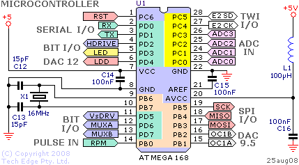
An Atmel Mega-168
RISC CPU U1 (Microcontroller) provides the unit's intelligence.
The Mega168 is a 28 pin device and a couple of analogue MUX devices are used to expand the
effective number of I/O pins. The M168 has 8 k words of 16 bit program memory, 1k byte of internal RAM
and 512 bytes of internal EEPROM memory. The TWI and SPI interface (described below) serve to
increase these limits and to provide interfaces to some of 2Y's other hardware devices.
A UART allows RS232 communication for logging and user interface functions.
The schematic shows the 16 Mhz crystal X1 (with oscillator capacitor C12 & C13),
decoupling capacitors C14, C15 & C16,
and inductor L1 for filtering the CPU's VCC, Analog VCC, and ADC references.
In the diagram the CPU's pins are colour coded - inside the block the ports B, C & D are
coloured alike. Outside the block the pin colours show how functions are grouped.
Of special note are the OC1A and OC1B outputs that are designed as PWM DACs with an
effective resolution of around 9.5 bits.
The DAC12 output also uses the SPI signals (MOSI, MISO & SCK) to interface the CPU
to the 12 bit hardware DAC on the lambda module.
Other control lines from the BIT-I/O group also go to the lambda module and other
points on the main board.
Six pins (RST, VCC, two GNDs, AREF & AVCC) are low level control inputs to the CPU.
Other points to note are that the 2Y PCB does not have an ISP (In System
Programming) header ).
This is because the ISP control lines are available on Y8 (the memory interface)
and the CPU is supplied pre-programmed and cannot be low level re-programmed without destroying the
special boot loader supplied with the unit (the boot loader is required to allow firmware upgrades).
Also, there is no rescue re-flash jumper - this is for two reasons; firstly we found way too many
people were trying to rescue re-flash when it was unnecessary and was usually counter productive, and
secondly a simple wire jumper can be used when rescue re-flash is required.
(refer to the diagram showing pins 5 and 16 connected with the red wire)
|
Power Supply, H+, Filtering & Power Cable
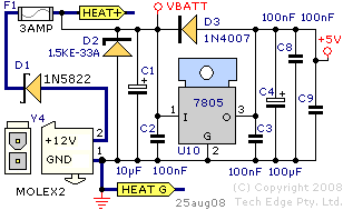
As well as the regulated +5 Volts used by the rest of the circuitry,
the power supply also provides the unregulated HEAT+ voltage that is
used by the wideband sensor (which is controlled by the pre-built lambda module).
PCB mounted 3 Amp fuse F1 provides protection against internally generated fault conditions.
Reverse polarity protection is provided by Schottky diode D1,
while fast Zener D2 (Tranzorb®) provides transient suppression.
Diode D3 protects the regulator (U10) from shorts across the battery input
where the regulator's output voltage, (supplied by C4) is higher than its input voltage.
Capacitors C1 through C4 filter and suppress electrical noise
around the 5 Volt 7805 (TO220) regulator U10.
C8 and C9 provide power supply bypass filtering for the
thermocouple amplifier, and lambda module described below.
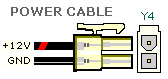
Molex MiniFit-Junior®
(connector Y4)
connects the unit to the mating power cable shown at right.
Note that prebuilt cables have the power conductor with the white flash connected to the GND pin.
Red heat shrink positively identifies the battery (+12V) connection.
Note carefully that the 2Y controller is designed to operate from a minimum voltage of (approx.) 10.5 Volts
to a maximum of (approx.) 19.5 Volts. The voltage limits are to protect the sensor from over current
damage.
Prebuilt 2.0 m power cables are available as spare part [20PWRCBL],
and Molex connector kits are available as spare part [PWRPLGK].
In operation the TO220 regulator (U10) does not dissipate much heat and sufficient heat sinking
is provided by the main PCB it bolts to.
Construction note: U10's M3 mounting bolt also secures one half of the
prebuilt lambda module via a spring washer and M3 nylon spacer screwed into the top of this bolt.
|
WB Module Connector, Transition PCB & Sensor Socket Y5
The 8 pin circular panel mount male socket Y5
connects the wideband unit to the sensor cable.
In the diagram, Y5's pins are colour coded according to the sensor cable's colours.
Y5 is soldered directly to the small
transition PCB
(it is labelled TE-SB).
The transition PCB is then connected to the main PCB with semi-flexible wires.
Note that the pins on Y5 are shown viewed from outside the case (NOT the solder side).
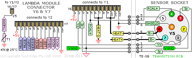
The 2Y pre-built lambda module uses a 0.1" spacing header Y6/7 with 25 pins to connect with
the main board and the sensor socket Y5. The signals to/from the lambda module are split into two sections
that interface directly with the wideband sensor (Y6), and to the microcontroller (Y7).
Note that the heater current carried in the HEAT- and HEATG circuits are split between
3 pins each of Y6 to minimise any problems associated with the high current carried through these pins.
All other circuits carry only small currents and a single pin therefore suffices.
The sensor's HEAT+ signals (also called H+) comes directly from the power supply section described above.
The thermistor T1, with nominal resistance of 47k at 25°C, allows the absolute on-board temperature
of the 2Y unit to be measured. This provide cold junction temperature measurement for software compensation (CJC)
for thermocouple readings.
Note that T1 is located near the thermocouple connector Y2 as this is the junction
temperature that is compensated for. Note that the thermistor is connected to pin-0 of Y7 (Y7p0) and this
is behind Y7p1 so that Y7 has an L shaped layout.
More information on the lambda module can be found here.
|
User & Thermocouple Input Muxing
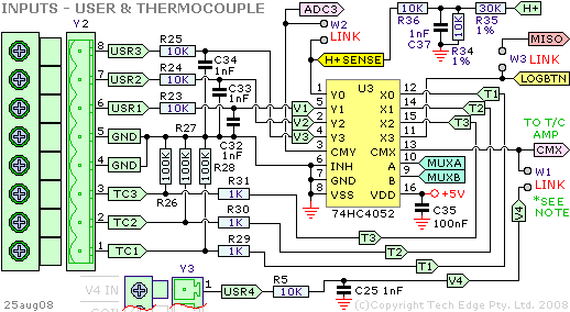
The 8 pin pluggable connector Y2
at the end of the case carries three thermocouple inputs (TC1 to TC3,
and three user voltage inputs (USER1 to USER3).
Note: this connector is reverse numbered from the right.
Additionally, pluggable connector Y3 carries
a single user input V4 IN (pin 10, rightmost on Y3) that is also on this circuit.
Note: V4 IN cannot be accessed
with the standard hardware, firmware and normal link settings.
Because we need more inputs than the microcontroller's 28 pins allows for,
a two section four channel multiplexer (MUX = 74HC4052) U3
is used to select 8 lines into two ADC converter inputs.
The MUX is controlled by lines MUXA & MUXB and the
MUX output CMY goes to processor input ADC3 and MUX CMX output goes to
the thermocouple amplifier described in the next section.
As well as the analogue user inputs,
The heater positive voltage H+ (see previous section)
is divided by 1% resistors R34 & R35, filtered by C37
to give H+SENSE.
This voltage is ¼ of the H+ voltage and H+SENSE is also an input into the USER side of the MUX.
The thermocouple side of the MUX also senses LOGBTN levels (see here).
six external analogue voltages into two ADC
input channels (ADC2 & ADC3).
Three channels are set up to sense K-type thermocouple inputs (TC1 to TC3)
and three 0 to 5 Volt analogue inputs USR1 to USR3.
Analogue user inputs USR1 to USR3 and H+SENSE have a very simple filter
comprising 1 nF bypass capacitors and 10 k input resistors.
The Thermocouple (and LOGBTN) inputs are filtered by the thermocouple amplifier described below.
|
Thermocouple (T/C) Amplifier & Option Links
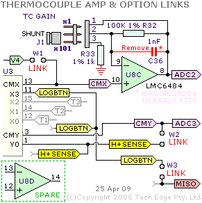
Op-amp U8C amplifies the signal from all thermocouples
(and the LOGBTN signal too, see previous section).
This amplifier is a compromise, and three individual thermocouple op-amps with
(+)ve and (-)ve inputs would have been better (but we only had a certain number of input pins).
C36, originally specified as 1 nF, was designed to provide some measure of thermocouple filtering.
*In April 2009 we decided to remove this capacitor because, even when made quite small, it stores enough charge
that it bleeds this through to the other channels (when in x101 mode) and corrupts their value.
Note: software processing also performs filtering of these signals.
The gain of the op-amp can be set at either 101 or, for redefining the T/C inputs into 0-5 Volt
User inputs, set to 1. But note that ALL the T/C inputs are affected by the gain setting, and
individual inputs cannot be selectively redefined like some of out other models.
Theory tells us gain is (R32+R33/R33) and with shunt J1 in the x1 position,
R32 is shorted so the gain is set to 1, or, when not shorted
(ie. J1 in x101 position) gain is 100+1/1 = 101.
The 101 gain stage results in a full scale 5.0 Volt input to the Mega-168 at a T/C input voltage of 5000/101 = 49.5 mVolt.
This K-Type table shows that 49.5 mV
corresponds to 1218 °C for the thermocouple.
In theory, changing R32 to a value larger than 100k will increase the gain,
and the same thermocouple can be used to cover a lower temperature range
(or a different type of thermocouple used), but remember if you do change
the gain, that logging or display software must be told of the non-standard settings.
Larger values of R32 may also cause gain instability so you may have to provide some signal filtering.
CJC: The T/C voltage is actually being measure between the
cold junction
(in the 2Y controller) and the hot junction at the thermocouple itself.
To calculate an absolute temperature the temperature of the 2Y's cold junction is measured with thermistor T1
and then this temperature is added to the computed thermocouple's raw temperature.
Thermistor T1 (see above) is physically located beside connector Y2.
T1 has a nominal resistance of 47k at 25°C and, with a simple calculation
(use this excel spreadsheet),
can measure absolute temperature of the board.
Cold junction compensation (CJC) may very important if K-type
thermocouples are used for low temperatures.
For example, for a thermocouple at 500°C, and a case temperature of 50°C,
without CJC the measured temperature would be 10% off.
Option Links:
There are three links on the board W1, W2 & W3.
In normal operation none of these links is fitted.
It is possible to build a minimal version of the controller by removing all the USER and TC inputs.
Further savings can be made by removing MUX chip U3 (described above), but to do this,
the W2 link must then route the H+SENSE signal to ADC3.
Link W1 can then route the V4 signal to ADC2
(V4 is the processed V4 IN signal from the Y3-pin 10 input.
This scheme allows a single user input to be read (it will be duplicated in the logging data stream).
Finally the W3 link should normally NOT be connected as the MISO
signal is critical to normal operation of the wideband unit, and its function cannot be modified
without firmware changes.
Note: No firmware changes are required if the above changes are made, and the standard
HXF file can be used.
Updates:
Note that U8 was originally specified as an MC33204 but,
for better thermocouple operation at room temperature and lower temperatures sensed by a K-type thermocouple,
we now use the better LMC6484 chip.
*As noted above C36 is removed to enable proper thermocouple operation (ie. for J1 in the x101 position).
More info here.
Accuracy:
Remember that the Mega-168 uses a 10 bit ADC converter (ie. 1024 levels over 1218°C input),
and in theory the best resolution is 1218/1024 ≈ 1.2°C.
In reality, without software averaging, one can expect at least 8 bits (256 different levels)
of accuracy for the ADC, and this results in about 4°C (≈7°F) resolution.
Software averaging can improve this figure, but it demonstrates the absolute accuracy,
and limitations, of the T/C inputs used on 2Y.
|
RPM Capture & Signal Processing
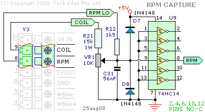
The Mega-168 has a number of useful hardware modules.
A 16 bit hardware counter is used to process time intervals with a 5 µSec. resolution.
The CPU's PB0 (ICP1) pin has an input capture function and this pin is driven
by the RPM signal from the circuit shown here.
Two input levels are available; a higher voltage designed to connect to the COIL primary of a
conventional points ignition system, and a lower level input designed to connect to the output of an ECU
(RPM input).
In the circuit C31, a 56 nF capacitor, is used as a high frequency bypass filter.
The preset variable resistor VR1 works with the capacitor to form a kind of
low pass RC filter.
Protection diodes D7 & D8 are designed to prevent damage to the IC.
U9 is a Schmitt trigger (six inputs) but only one input is actually used.
It should be carefully noted that end
connector Y2-pin 4,
which was also used for the original
2A0 and 2A1 controllers, may be printed with the words RPM.
The only RPM inputs are actually on Y3 as noted in the diagram,
so if your end-plate does have RPM printed there, please remove it (as the input is actually grounded!).
Accuracy & Conversion:
The Mega-168 converts the RPM data into a count of 5 µSec time periods that is averaged over two
successive RPM pulses. To convert this count to something useful, first assume we are looking at pulses
from a 4 cylinder 4-stroke motor that produces two pulses per revolution (ie. PPR = 2.0).
At 2,400 RPM there will be 2400/60 = 40 revs/sec or 80 pulses/sec.
As each second is made up of 1,000,000/5 = 200,000 count periods, there will be a count of 200,000/80 = 2,500.
So, a count of 2,500 corresponds to an RPM of 2,400.
The generic formula is:
- ⇒ RPM = 12,000,000/(count * PPR)
- ∴ count = 12,000,000/(RPM * PPR)
Higher revs produce smaller counts, and the lowest RPM that can be recorded (4 cyl.., 4-stroke) for the 16 bit
count field is 65,535 and this is 91.6 RPM - which is barely cranking speed for modern motors.
At high RPM and high PPR rates the pulse frequency increases.
The hardware low pass filter will start take effect at very high RPM and pulses will not be recorded
accurately - in this case reducing C31's value may help (but possibly at the expense
of more noise at lower RPMs).
Quantisation Error: At high RPMs the lumpiness of the 5 µSec time intervals becomes apparent.
At 8,000 RPM for a 4 cyl. engine (PPR = 2) the count will be 12,000,000/16,000 = 750.
The next count, 751, would be recorded as an RPM of 12,000,000/(751*2) ≈ 7,989 RPM.
So at 8,000 RPM the resolution is 11 RPM - at lower revs the resolution improves, and at higher
PPR values (ie. for 6 and 8 cylinder engines) the resolution degrades.
|
Wideband Outputs - WBlin+/-, NBsim & SVout
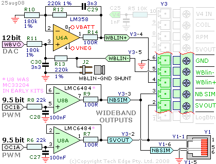
Three voltage outputs are provided.
One high quality differential WBlin+/- output is generated on the lambda module
by the 12 bit hardware DAC (WBVOUT circuit on Y7-p9).
WBVOUT is amplified (see below) and filtered by U6A (LM358) and is output on the WBLIN+ line.
The WBLIN- circuit is actually an input, and when the J2 shunt (WBLIN-GND)
is OFF the, WBLIN+ output will be lifted (or reduced) by the voltage on the WBLIN- input.
We call this a differential output and the concept behind it is discussed
further here.
An important aspect of the differential WBlin driver is the negative bias voltage V NEG
required to ensure WBlin+ can track both positive and negative changes on the WBlin- input.
This bias is obtained from the RS232 chip U5 described in the RS232 section.
Note that WBlin- should not vary by more than +/- a few volts from the GND value (say +/- 3 Volts).
If you leave WBlin- to float (ie. with the WBLIN-GND shunt removed) then WBlin+ could float up
to VBatt, forcing WBlin+ to be at a considerably higher voltage than most devices connected to it will expect.
Remember also that if you connect a current device (something like a direct reading milliAmp meter)
across WBlin+ and WBlin-, then the WBlin- jumper should also be connected to avoid both WBlin+ and
WBlin- floating up to VBatt and cutting off all current.
The 12 bit DAC (DAC7612 on the lambda module), with an accurate internal reference,
generates voltages in steps of exactly 1.0 mV.
U6A is wired as a differential amplifier with bias correction
and has a gain of 220/180) and gives WBlin a maximum value of 4.095*220/180 = 5.005 Volts
in steps of ≈1.22 mVolts.
Note the 100 Ohm resistor R14 is used to limit short circuit output current and
is wired in the feedback loop to avoid changes in the output voltage when
low impedance loads are used.
The CPU's OC1A & OC1B outputs are set up as two 10 bit PWM generators.
A simple single pole filter, using op-amp sections U8A & U8B
adds some smoothing and filtering to each output.
In practise this results in the SVout and NBsim signals
having somewhat less than the 10 bits of PWM resolution available, so we have called each
PWM circuit a 9.5 bit DAC.
All outputs are available on pluggable
connector Y3.
The single ended outputs NBSIM and SVOUT (along with GROUND) are also available on
Y1A & Y1B
|
Interface (TWI + SPI) & On-Board Logging Button(s)
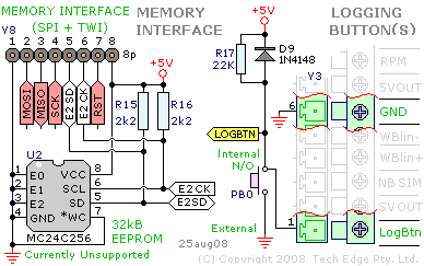 The Mega-168 has only small amounts of non-volatile memory but external memory (called on-board logging memory)
can be used to store AFR and other data sensed through the input channels.
There are two memory interface busses the I2C bus
(Atmel calls this the Two Wire Interface or TWI)
and the faster serial Peripheral Interface bus or SPI bus.
Both these busses as well as 5 Volt power, GND and the processor RESET lines go to
the memory interface connector Y8.
The TWI bus also connects to an 8 pin dip socket wired to interface to an
ST-M24256-B
256 kbit (32 kbyte) EEPROM.
Note: Current firmware does NOT support the TWI memory interface
The Mega-168 has only small amounts of non-volatile memory but external memory (called on-board logging memory)
can be used to store AFR and other data sensed through the input channels.
There are two memory interface busses the I2C bus
(Atmel calls this the Two Wire Interface or TWI)
and the faster serial Peripheral Interface bus or SPI bus.
Both these busses as well as 5 Volt power, GND and the processor RESET lines go to
the memory interface connector Y8.
The TWI bus also connects to an 8 pin dip socket wired to interface to an
ST-M24256-B
256 kbit (32 kbyte) EEPROM.
Note: Current firmware does NOT support the TWI memory interface
The on-board memory is used to store data when on-board logging is active.
The two 2.2 k resistor are the required pullup for the TWI SCL and SDA lines.
A 100,000 programing cycle & 40 year data retention is claimed for the device.
On-board logging is controlled by press-button switch PB0
(refer to logger details here).
Components R17 and D9 interface the switch to the processor and
provide a small amount of protection for the mux U3 (not shown) that the LOGBTN signal connects to.
|
1 Megabyte Flash Logger Module
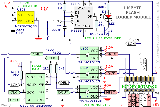 The 1 Mbyte Flash Logger Module
is a simple plug-in board that adds
the on-board capability to save all logged data for later retrieval by a PC.
The module connects to 2Y's memory interface (previous section).
The module uses the SPI interface lines for writing and reading the flash memory
and also the TWI lines (in bit set/reset mode) to control the flash part.
Note that the TWI interface cannot be used (in I2C mode)
with the 1 Mbyte module plugged in (and besides, current firmware does not yet support the TWI mode).
The 1 Mbyte Flash Logger Module
is a simple plug-in board that adds
the on-board capability to save all logged data for later retrieval by a PC.
The module connects to 2Y's memory interface (previous section).
The module uses the SPI interface lines for writing and reading the flash memory
and also the TWI lines (in bit set/reset mode) to control the flash part.
Note that the TWI interface cannot be used (in I2C mode)
with the 1 Mbyte module plugged in (and besides, current firmware does not yet support the TWI mode).
The logger circuit, which uses a 3.3 Volt
SST flash
part U602, must be interfaced to the microcontroller's 5 Volt bus.
The two HC single gate buffers (U603 & U604)
and an HCT gate (U605)
Provide two-way level conversion for the SPI Signals.
This scheme ensures reliable high speed operation as compared to a simpler scheme using resistors.
The U606 NE555
pulse/timer device, wired as a
monostable, provides pulse extension
of the Data ENable (DEN) signal so operation of the module can be seen as a flashing
of the surface mount LED D1.
Note the E2CK signal, as defined on the logger module, changes to DEN (Data ENable)
and E2SD changes to LCH (LatCH). This is to more correctly identify the TWI
lines as being used in a simple bit toggle mode.
|
Indicator LEDs & External 5 volt Power Supply
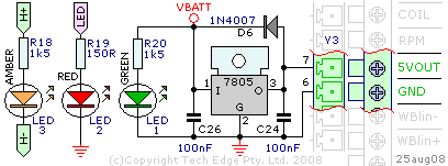
2Y adds a regulated 5 Volt supply for external device power that can be used for sensors (like MAP, TPS, etc.).
The regulator U12 operates like U10 that supplies power to the main circuit.
As only limited heat sinking is available on the main board keep current drawn from this regulator
to 200 mA or less (although a larger current can be handled by the regulator, it will thermally limit if overloaded).
The three LEDs and current limiting resistors R18, R19 & R20 are mounted
beside the logging button PB0.
The green LED1 is a simple power monitor and should always be lit when power is supplied to the unit.
The red LED2 is the main diagnostic device when the controller is in operation,
and will show various faults that can be detected,
and also logging status (refer to the 2Y User Manual for more details).
The amber LED3 is wired across the heater power circuit and can be used as a good diagnostic aid.
Sensor cable faults, low voltage power supply, and other conditions will cause the
amber LED to flash irregularly and weakly, whereas a normally powered sensor
will be shown by a healthy, faintly flickering LED.
|
RS232 Driver, Splitter, (-)ve Generator, Y1A & Y1B
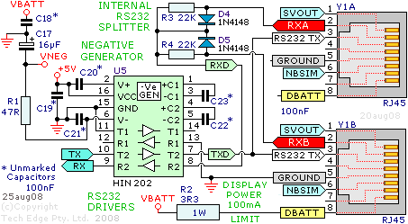 The serial driver chip U5 (HIN202) includes a charge pump circuit to produce a true negative RS232 rail.
This (-)ve voltage is also available externally (p6 V-) and is used to generate a bias for the WBlin+/WBlin- driver circuit described above.
Y1A & Y1B
are standard RJ45 connectors that carry the RS232 Rx, Tx and common GROUND return signals.
To avoid signal contention on the incoming Rx lines
(where two different external devices could have their Tx lines shorted to GND)
the components R3, R4, D4 & D5 provide the necessary protection.
The serial driver chip U5 (HIN202) includes a charge pump circuit to produce a true negative RS232 rail.
This (-)ve voltage is also available externally (p6 V-) and is used to generate a bias for the WBlin+/WBlin- driver circuit described above.
Y1A & Y1B
are standard RJ45 connectors that carry the RS232 Rx, Tx and common GROUND return signals.
To avoid signal contention on the incoming Rx lines
(where two different external devices could have their Tx lines shorted to GND)
the components R3, R4, D4 & D5 provide the necessary protection.
As the RJ45 connector is a non-standard pin-out, a special adaptor cable is required
for connecting the device to a PC or other logging, display, or control device (see RS232 Data Cable below).
The DBATT point provides connected devices with a current limited source of power and is used
by various displays. Note: as the current is limited by a 3.3 Ohm resistor,
a short across DBATT to GND will result in up to 4 Amps of current - this will be enough
to cause the 1 Watt resistor R2 (dissipating 50 Watts) to overheat in a few seconds.
This short-circuit current may not be enough current to blow the internal 3 Amp fuse
but it may be enough to eventually vapourise the PCB's track to R2.
Y1A & Y1B also brings out the NBSIM & SVOUT
analogue signals (SVout is for compatibility with older displays like the LD01 and TE-5301,
but note that the TE-5301 has a DB9 connector,
and will note mate directly with Y1).

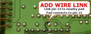
Updates: Note that the Rev 1.0 PCB has an artwork error and a
wire link (click for large image)
must be added between pin 13 and GND of U5 (on the underside of the PCB).
This modification electrically connects pin-13 to pin-15 of U5 although the physical fix connects pin-13 to an adjacent earth pad (which is connected to pin-15).
|
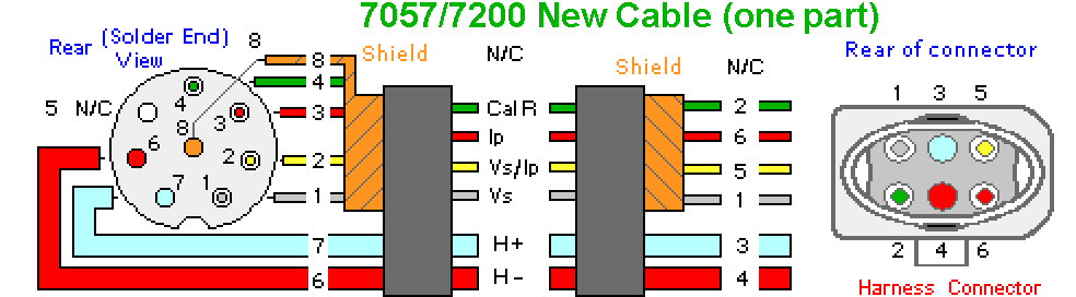
Sensor Cables (7200/07057, 6066, 17025 & L1H1)
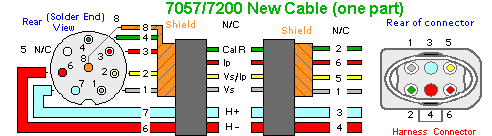
This cable connects the wideband unit to the sensor.
Specifically, the cable is from 2Y's circular 8 pin connector
(Y5)
to the sensor.
The schematic shown is for the 7200/7057 sensor.
Also available are very detailed schematics and images of
other WBo2 cables.
Shown here is a 7200/7057 connector
with attached cable.
Here is the main cable construction page
and much information about the actual connectors is on
this page
|
Serial (RS232) Cable = WB-PC cable
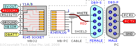
The serial (or RS232) data cable is an external cable that plugs in to one of
the two RJ45 connectors (Y1A or Y1B)
at the side and sensor/power connector end of the 2Y unit.
The cable has two wires and a shield that acts as a third common wire.
Here's an image of the RJ45 end of the cable
and detail of just the DB9 end of the cable.
In the above image the RJ45 socket (left) is on the 2Y unit,
the rightmost male DB9-P (plug) is the connector at the back of a PC.
Remember that the face of all DB9 connectors carries the pin numbers (so you don't have to guess).
The DB9-S (socket) is the female end which is on the cable itself.
The clear RJ45 crimp-connector is the same plug used for Ethernet cables and
can be crimped with the same tool. In the schematic above:
- The red wire carries an incoming RS232 level signal from an external
device. This wire typically carries commands to the wideband unit.
-
The white wire carries signals from the wideband unit.
Note that at the wideband end the white wire is called RS232 Tx
but at the other end it is called PC Rx - this reflects
a user's differing view of reality; at the wideband end (Tx) and at the PC end (Rx).
- The shield is the common return wire for the Rx and Tx signals.
It is designed to limit interference or noise being injected into the wideband unit.
It goes to pin 5 on both connectors.
Here's what's in the DB9 connector kit
which is available as spare part [DB9FKIT].
Pre-built RS232 cables (1.2 m long) are available as spare part [12RS232].
For PDA use (ie. Palm, etc.) a different cable connection is required.
Refer to the Palm Logging page for more information.
|
Four Digit 7 Segment Display Option (not used in 2Y1)
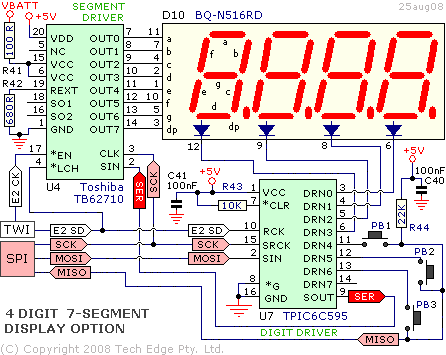

Note: This option is not available with currently available 2Y1 kits as we cannot obtain the high-side driver U4 as a through hole component.
We hope to offer an updated 2Y kit with an alternative driver chip in the future.
The four digit 7-segment common cathode display module D10 (BQ-N516RD) is driven
by high side segment driver U4 (TB62710)
and low side digit driver U7 (TPIC6C595).
The driver chips are controlled by the processor's TWI & SPI lines.
The SPI lines, used in bit set/reset mode clock, serially transfer data into both driver chips.
Note that U4 receives its serial data from U10 on the SER line -
this scheme allows a single data stream (on MOSI) to filter through a number of chips
(so, U4's SO1 output could be cascaded to another chip).
The TWI lines E2CK & E2SD are also used in bit set mode to
transfer the latched data to the driver outputs (note that U4 requires two driver lines to operate
glitch free).
Low side driver U7 is a very high current HexFET switch and is set to sequentially
select outputs DRN0 to DRN3 that drive each of the 4 digits. Only one digit is selected at one time
and very little power is dissipated by this chip due to its low ON impedance.
High side driver U4 drives each digit-segment (a through g & dp)
at a constant current (and thus constant brightness).
The segment current is determined by the external resistor R42 but the power is actually
dissipated in U4, and you will note that this chip will normally be a little warmer than other ICs.
To help share power dissipation, resistor R41 connects the segment power line
(VCC) to VBATT and its value is designed so it also gets a little warm.
The display's brightness can still be changed by controlling how long the digits are enabled
(see E2CK into U4's *EN line).
U7's outputs DRN4 to DRN6 (DRN7 is not used) can
be used to sense switch presses from on-board buttons PB1 to PB3.
The MISO line is used to sense if a button is pressed or not, and
pullup resistor R44 ensures a logic high level when no button is pressed.
Note 1: Using MOSI in this fashion means it cannot be used as a data input from SPI logging memory.
Note 2: Using E2CK to drive U4's *EN also means it cannot be used to read TWI logging memory.
|
We appreciate your feedback on the content and any corrections necessary to this article.
|
)
)
)
)
)
)
)
)
)
)
)
)
)