![]() |
| ![]() Buy
| WBo2
Buy
| WBo2 ![]() | 2E0
| DIY 2E0 Kit
| Construction Guide
| Location Guide
| Schematics
| Test Procedure
| 2E0
| DIY 2E0 Kit
| Construction Guide
| Location Guide
| Schematics
| Test Procedure
Here are notes and schematics to help you understand how the TE-WB Version 2E0 works. Please note that all images and text are Copyright 2005 © Tech Edge Pty. Ltd.
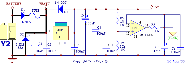
Battery power is connected to the unit via Molex Minifit 90° PCB mount socket Y2. Reverse polarity protection to the unit is provided by Schottky diode D1, while fast Zener D2 (Transorb) provides transient suppression. The PCB mounted 3 Amp fuse provides protection against internally generated fault conditions. C1 through C4 filter and suppress vehicle electrical noise around the 5 volt 7805 (U10 D2PAK) regulator (mounted on the solder side of the PCB). Diode D3 protects the regulator from shorts across the battery input. Op-Amp U8D (MC33204) generates a 2.0 V Virtual Ground (VGND) which is used as the reference point for the analogue interface to the sensor. C5 and C6 provide filtering and noise suppression while R7 provides short circuit protection in the event of a fault. |
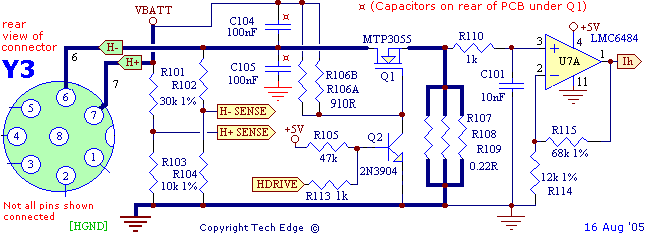
R101 to R104 constitute two voltage dividers to sense the H+ & H- heater voltage. These voltages are fed to the muxes (see 74HC4052 mux sections below). Heater current is sensed by measuring the voltage developed across resistors R107 to R109. U7A amplifies and filters this voltage to produce signal Ih. FET Q1 switches on and off at 30 Hz (ie. PWM control) to control the average current to the heater. The gate drive transistor Q4 is controlled by the microcontroller and ensures the FET switches quickly and cleanly. C104 and C105 (attached under Q1 on the solder side of the PCB) provide a path for switching transient currents and work to reduce the effect of the large heater switching transients and induced voltages on sensitive parts of the circuit. |
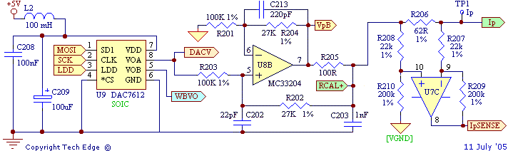
The sensor is an analogue device but it is controlled by digital signals. The 12 bit dual DAC (Digital to Analogue Converter, DAC7612) produces a voltage in the range of 0 to 4.096 volts (in steps of 1 mVolt). The DAC's A section output is buffered by op-amp U8B and then applied to the sensor's Ip drive to produce a pump current which flows though resistors R205 and R206. This arrangement gives an Ip Voltage of +/- 2.0 Volts (relative to VGND) and this provides the positive or negative pump current to control the sensor's pump cell in the rich and lean regions. The B section of the DAC drives the linear wideband output WBLin (see section output below). The DAC's power supply is decoupled from the other digital circuitry via Inductor (L2) and capacitors C208 & C209. The DAC is an SPI device (see microcontroller section below). The pump cell is a current operated device and the Ip generated by the DAC's output voltage is calculated by measuring the voltage developed across 62 ohm sense resistor R206. For the LSU sensor, its calibration resistor acts in parallel with R206 (shunt J2 must be in the 2-3 position). Differential amplifier U7 senses the pump current and produces a voltage IpSense. |
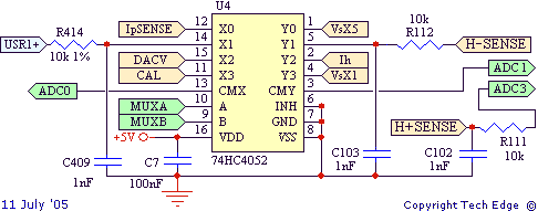
The dual 4 to 1 line mux U4 (74HC4052) allows two groups of four signals to be sensed by the microcontroller's two ADC input lines ADC0 and ADC1. Wideband signals Vsx5, Ih, Vsx1, IpSense, DACV & Cal (VGND) voltages are sensed as well as H- via filtering provided by R112 and C103. also shown here is the H+ sense signal but it is not selected by the mux, but rather passed directly to the microcontroller via filter components R111 and C102. Analogue user channel 1 USR1 (see Y5 connector input below) is also sensed by this mux. |
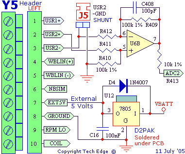
10 pin I/O connector Y5 with screwable plug-in header is on the long side of the case beside the amber heater LED. It carries both inputs, outputs and a separate 5 Volt supply for powering sensors. The header signals, described from the connector's left, are as follows :
Analogue user input USR2 is differential and is amplified by U6B with filtering component C408. Shunt J5 should be ON when just the USR2+ signal is connected to a signal source. For full differential operation, J5 should be OFF and the USR2- input connected to the ground point near the signal source. The 5 Volt regulator U12 is a D2PAK device and is solder under the PCB. The pin 2 connection goes to the D2PAK's tab. Diode D4 protect the regulator should it be connected to battery positive. Internal protection circuitry within the regulator shuts it off in the event of overload or a short. |
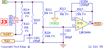
The Vs Drive (VsDRV) signal is used to sense the impedance (know as Ri) of the Vs Sense cell. As the LSU (Bosch) and the L1H1 (NTK) Vs cells have very different characteristics, a different mechanism is employed for controlling the heater of the NTK sensor. For the NTK sensor, the LSU's 910 ohm resistor changes to 82 k by use of jumper shunt J3. The LSU position for J3 is 2-3. Note the warnings elsewhere about using the wrong J3 position with a given sensor which can cause damage to the sensor. |
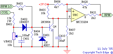
The RPM capture circuit takes a pulse signal from either the COIL or RPM LO connector. The COIL pulse signal passes through a voltage divider (R401, VR402) and a variable high pass filter with C401 as the high frequency shunt component. The alternate low voltage input is applied directly to transistor Q4's base. Diode D401 steers the signal between the two inputs and D402 protects Q4 against reverse voltage pulses. Q4 acts as an amplifier and decoupling component between the inputs and the Schmitt trigger U8C. The conditioned RPM signal is sent to the microcontroller's input capture (ICP) pin. |
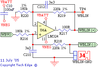
The microcontroller (CPU) processes the IpSense signal in software to produce a WBlin software count. The second section of the 12 bit DAC (see above) generates up to 4.096 Volts. U6A has a gain of 220/180 and gives WBlin a maximum value of 5.006 Volts (4.096*220/180) in steps of 1.2 mVolts. Note the 100 ohm resistor R217 is used to limit short circuit output current and is wired in the feedback loop to avoid changes in the output voltage when low impedance loads are used. The WBlin- signal is a voltage reference for the U6A op-amp circuit which is powered from VBATT and a negative rail derived from the RS232 driver chip (described below). The WBlin+ output is raised or lowered relative to this reference but this voltage is ultimately limited by the op-amp's power rails. Capacitors C210 & C212 are the filter elements of a two pole Sallen-Key filter. Jumper shunt J4 provides a default ground reference for the output and should be removed when the floating output is required, but remember that if WBlin- is left to float then the WBlin+ output will also float and become meaningless. |
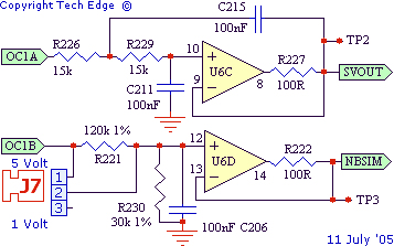
The CPU's 10 bit PWM generators (OC1A & OC1B) are used to produce the SVout and NBsim signals. Op-amp sections U6C & U6D buffer these signals. A simple single pole filter adds some smoothing and filtering to the NBsim output. A more complex double pole Sallen-Key filters smooths the SVout signal. The NBSim output has a special feature. Normally, with the J7 jumper in the 1-2 position, the output is programmed in the range of 0 to 1 Volts. By placing J7 in the 2-3 position, the output will be divided by 5. To compensate, the NBsim output should be reprogrammed to the 0-5 Volt range. The advantage is that better resolution (more steps between adjacent voltage levels) is achieved. |
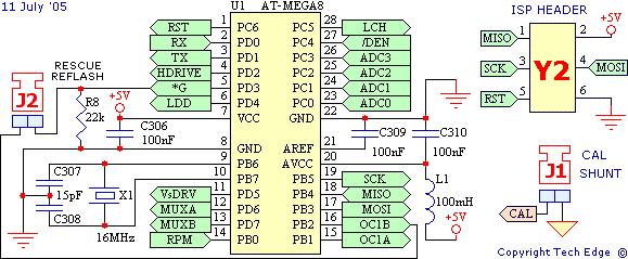
An Atmel Mega-8 (16 Mhz) RISC CPU provides the unit's intelligence. The schematic shows the crystal, decoupling capacitors, and the inductor for filtering the CPU's analogue ADC reference. Rescue-Reflash jumper J2 is provided to enable a hard reflash in the rare occasion when main program memory has been corrupted. The ISP (In System Programming) header is use for factory programming and testing. The calibration jumper J1 is also used for factory testing, and should remain in place for all normal operation. |
3 Digit LED ReadoutThe 3 digit LED display PCB is attached to the end of 2E0's main PCB. An 8 pin 90 degree header (shown in light blue at left) with 0.1" pin spacing is used on the Main PCB. The LED PCB has a matching set of unprotected pins. The pins are numbered from right (left pin is #8) when looking at the silk screening on the LED PCB. As described below, the display is driven by 5 processor signals and is provided with power from Vbatt, +5Volts and GND. An on-board D2PAK SMD regulator supplies power from the Vbatt line. Jumpers are provided to power the display directly from the 5 Volt main rail (but this option is not used). The display LED circuitry is broken into two diagrams shown below. |
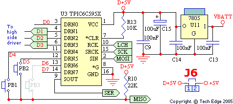
The first is of U3, the low side (or sink) driver using a TPIC6C595 which drives the LED common cathode 7 segment displays. This chip has a low ON impedance of less than 7 ohms and is ideal for the purpose. CPU signals SCK (clock) and MOSI (data) clock data into the '595. The LCH (processor PC5) then latches the data to replace the previous data. Note that only 3 of the 8 outputs are used to drive the LED cathodes. PB1 & PB2 are regularly poled to determine if one of these buttons is pressed, which pulls the MISO line low. The 22k R10 terminates MISO high when neither button is pressed. The 5 Volt SMD D2PAK regulator U11 is wired to only provide power to the LED PCB. Jumper link J6 must NOT be wired so just the on-board U11 regulator powers the display. |
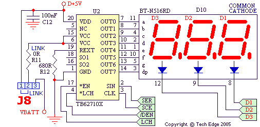
The next diagram is of U2 the high side (or source) driver circuit using the Toshiba TB62710P. This chip sources current for the LEDs with 680 ohm R12 selecting the desired LED current. The same serial interface signals SCK, MOSI & LCH are used, and the additional /DEN (processor PC4) allows the display to be disabled. The J8 wire link jumper connects pins 1 - 2 so U2's power circuitry is driven from the on-board 5 Volt regulator. Note also that R11 is actually a zero ohm link. R11 could have been used to dissipate some power if the VBatt power connection (link 2-3 on J8) had been selected. |
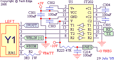
The serial driver (ST202) includes a charge pump device to produce a true (-)ve RS232 rail. Y1 is an RJ45 connector and requires an adapter cable for connection to a PC or Palm (see RS232 Data Cable below). Y1 also brings out the narrowband, wideband (+ differential output only) and SVout (for the display) analogue signals. An external splitter board is available that splits the single RJ45 into two and (one for the display and another for a serial connector) as well as providing dedicated connectors for WBlin and NBsim signals. |
Sensor Connector & Spare Op-Amps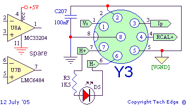
The sensor connector Y3 (previously described above) carries the control signals to and from the 5 wire pump cell, as well as the heater's H+ & H- signals. C207 filters noise between the analogue ground (VGND) and the power GND signals. The standard unit to sensor cable has a shield (pin 8 of the cable) around the Vs, Ip & Vs/Ip common wires. Note that pins 2 and 5 of Y3 are connected together to remain compatible with rev 1.0 and 1.5 WBo2 controllers. The amber LED D5 provides a measure of power supplied to the sensor's heater, while R3 limits current though the LED. The controller has a couple of spare op-amps - U7B & U8A. |
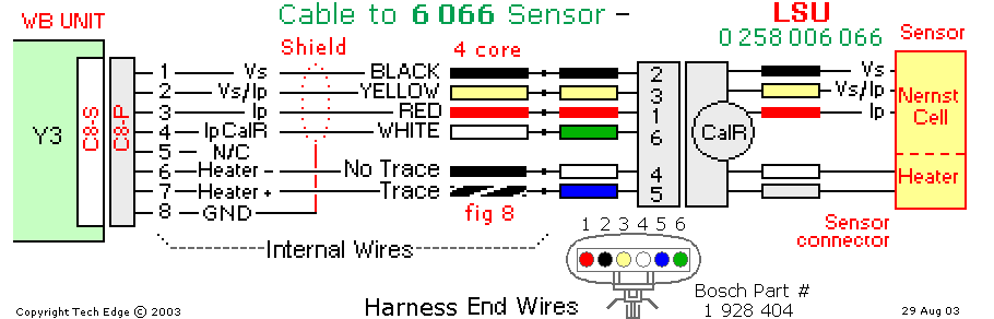
This is the cable from the circular 8 pin connector (female end of Y3) to the LSU sensor connector. The connector shown is for the 0 258 006 066 sensor. See also the LSU information page with pinouts for other LSU sensors and the NTK (L1H1) sensor cable pages. |
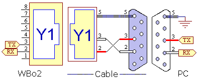
This is the serial data cable from the RJ45 connector (female end of Y1) to the RS232 DB9 connector. The red wire carries commands from the external device (PC, etc) and the white wire carries logging data and responses from the WB unit itself. For PDA use (ie. Palm, etc.) a different cable connection is required. Refer to the Palm Logging page for more information. |
We appreciate your feedback on the content and any corrections necessary to this article.