![]() |
| ![]() Buy
| WBo2
Buy
| WBo2 ![]() | 2E0
| DIY 2E0 Kit
| Construction Guide
| Location Guide
| Schematics
| Test Procedure
| 2E0
| DIY 2E0 Kit
| Construction Guide
| Location Guide
| Schematics
| Test Procedure
|
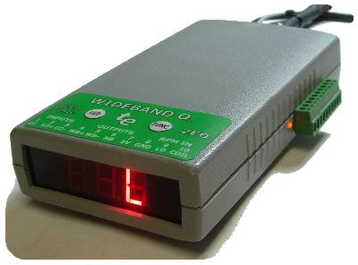
(updated 25 April '06) -- These notes are designed to help you construct your own 2E0 WBo2 Bosch LSU4 / NTK L1H1 oxygen sensor interface unit. As noted in the location guide, Many of the images below can be enlarged by clicking on them. Links in red are JavaScript pop-up images. |
|
Certain skills are requires to construct this kit successfully, and then to test and debug should there be any problems. Tech Edge provides the kit in good faith, and offers a warranty repair service where you pay us to fix a kit you couldn't get working. |
|
We're also happy to replace components that are DOA (dead on arrival) as we don't 100% test parts supplied to us. |
|
Faulty components are rare but do happen, but we don't automatically replace parts damaged by static electricity (ie. zapped). |
|
We do NOT offer a refund of any kind on fully or partially completed kits. If you find the construction task too daunting then you can return your unopened DIY kit for replacement with a pre-built unit (along with a price adjustment of course). |
Remember to look at the Yahoo oz-diy-wb list for answers to questions. We appreciate feedback and actively update guides, such as this page, in response. When you see the warning symbol (at left), it denotes that special care should be taken with this step.
We suggest you read all of this guide before commencing construction to avoid painting yourself into a corner by completing a step before it should be, or using one part where another should be used.
|
Firstly inspect your bare PCB for any shorts between adjacent tracks. Our PCBs are 100% tested so there should be no problems of this nature but it's best to find any board faults before you've built the unit. |
If you haven't already done so, you should go here and print off component location image(s). In particular, print off the component location guide.
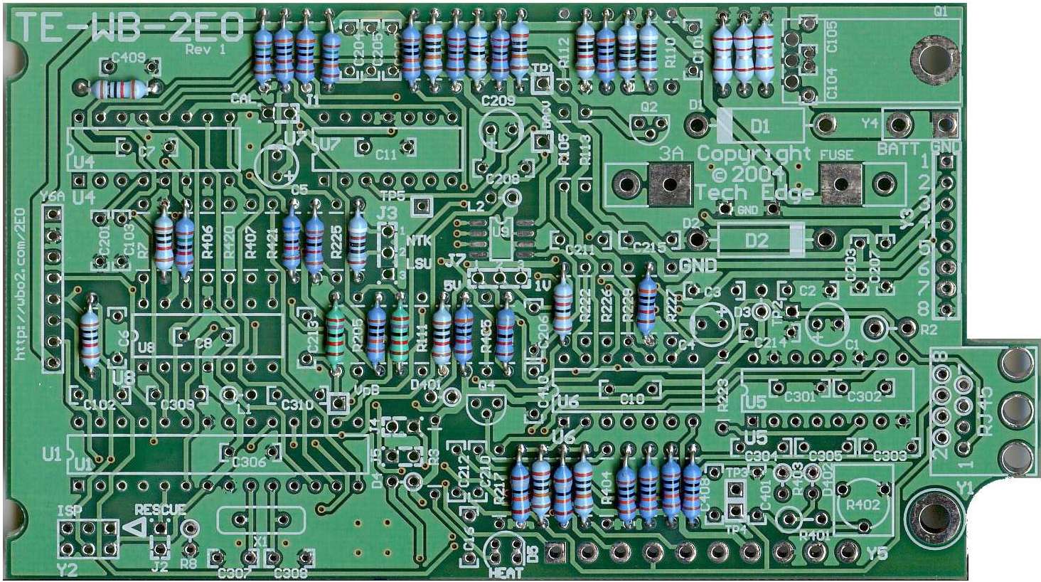
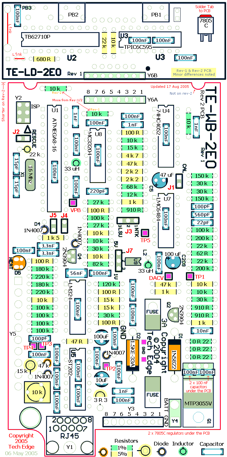
Getting StartedThe silkscreen has visual cues for using 1% or 5% resistors. The 1% resistors having a dotted line as shown in the blowup at right. 5% Resistors are also marked in yellow on the color component overlay, while 1% Resistors are marked as Green 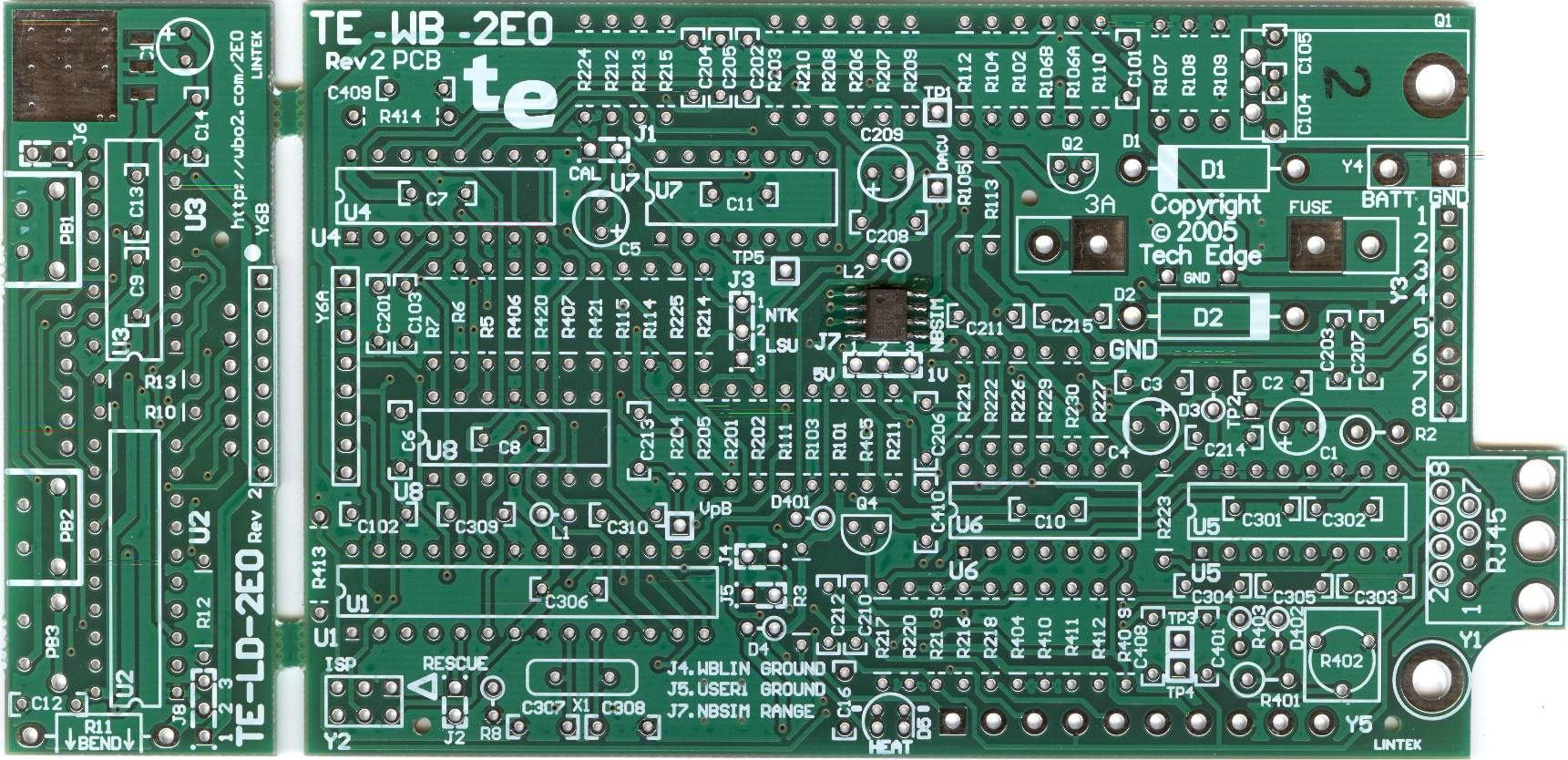
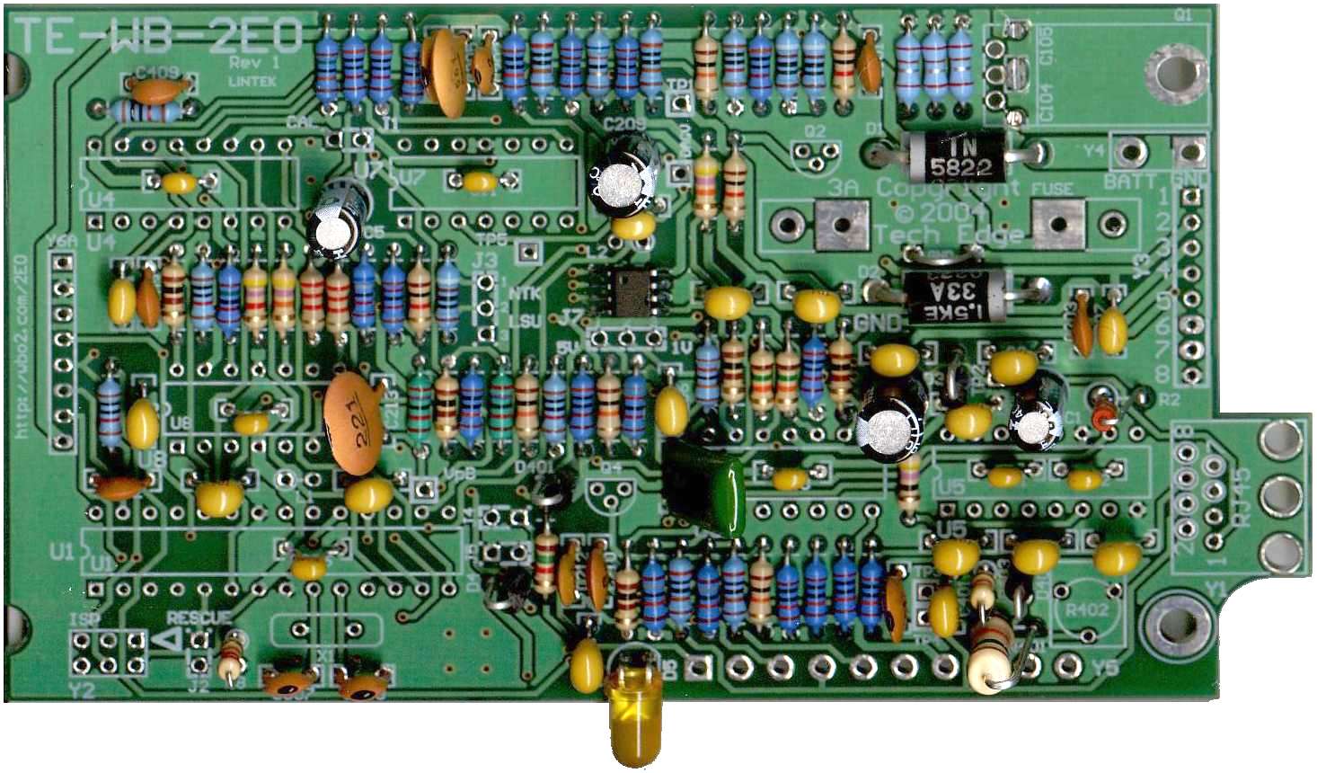
This shows the complete bare board including the LED PCB at the left. Not shown is the third transition PCB for connection of the circular PCB to the main PCB. Not all the PCB images shown here show the SMD (surface mount) 8 pin DAC soldered to the centre of the main PCBs in all kits. The image at left DOES show the DAC. Click on the image for a x4 enlargement. Note that these image files can be large and are from 150 to 300 k in size depending on magnification. Resistors - 1% & 5% and Their Substitution
It is important that 5% resistors are not used where a 1% resistors is called for. But it's okay to use a better 1% resistor in place of a 5%. We may actually substitute with a 1% for a 5% part in the parts kit from time to time, but we will never substitute with a 5% for a 1%. Note : Resistors, in the kits, are marked in text on the paper reel without the k (indicating 1,000). Thus, 20 means 20 k. But, resistors less than 1 k are marked with an R, so 910 ohms is marked as 910 R. However, measure all resistors before using them to check we have not made a mistake, or you have not misunderstood our marking scheme. If you end up with a resistor of the wrong value after installing most, then there's a chance one you previously installed was the wrong value. |
1% 1/4 Watt ResistorsFirst we insert the physically lowest components - these are the 1/4 watt resistors. We install the 1% resistors first as these are more numerous. The 1% resistors have a light blue (or light green) body. They have 5 coloured bands - with one end being red to indicate the 1% tolerance. It's advisable to orient the resistors so they have the red bands to the top and the right to make it easier to read should you need to check any resistors at a future time. |
|
|
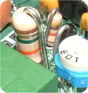
5% 1/4 Watt ResistorsNext the 5% resistors go in. 5% resistors typically have a beige or light brown background. It's best to orient them with the gold band to the right and to the top. Note that the three 0.22 ohms resistors (top mid right, very light blue) may be supplied as either 2% with a red band rather than brown (most likely), or in some instances, as a 5% (with standard gold band). Note that three 5% resistors are installed vertically. The image at left shows them laying flat on the PCB with white circles around for easy identification. They are R2, R8 & R403. |
|
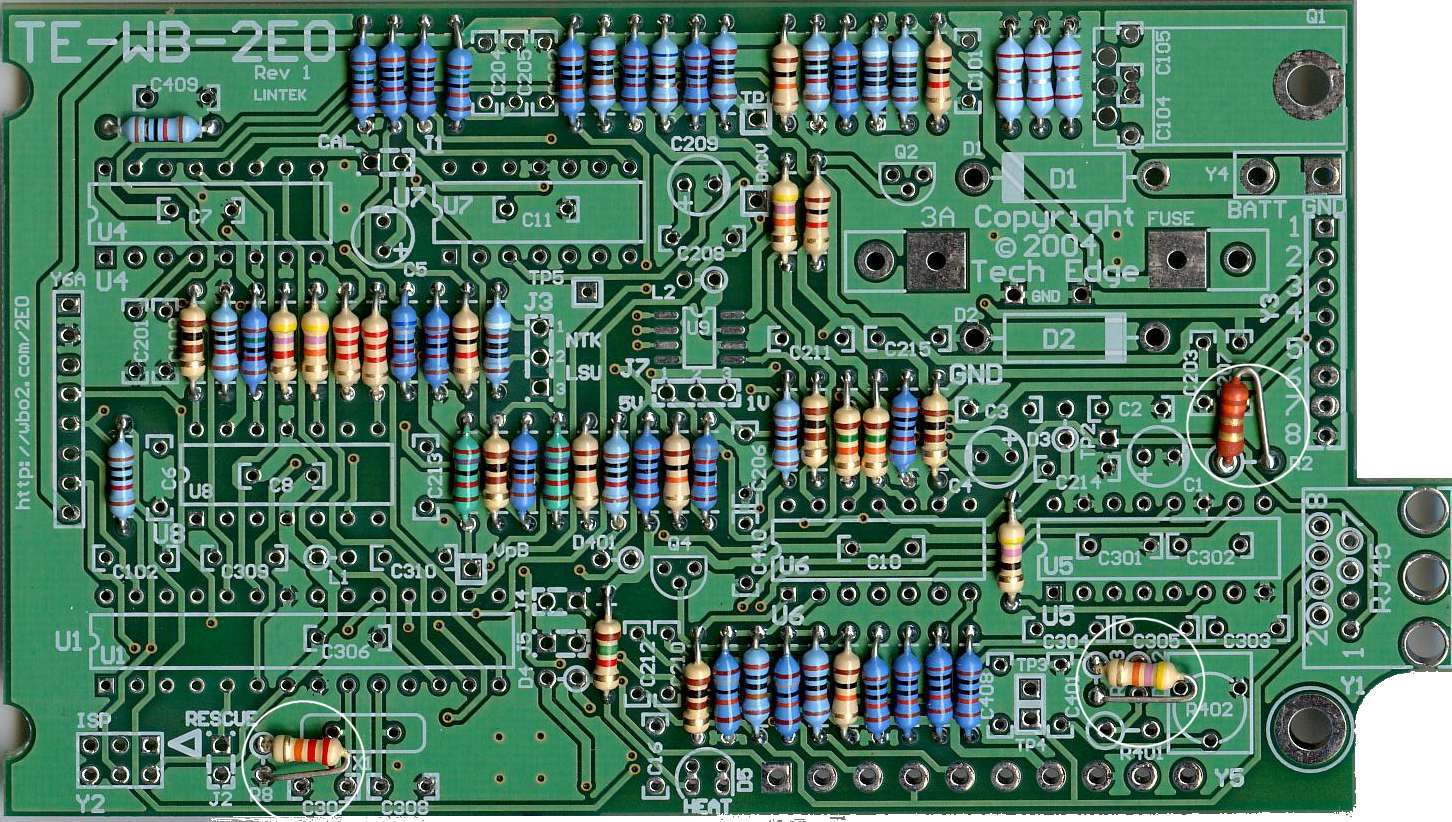
Also, only for these vertical components, the PCB overlay's circle and straight line suggests the way the resistor is inserted with its main body closest to the circle, and the longer wire to the straight line. 5% 1 Watt ResistorR401 (= 15k 1W) is the large resistor outline in the lower right corner beside the trimpot and green connector. This resistor can probably be left until later to install, as it sits much higher than other parts. It's mentioned here to complete the resistor section and is shown at right. At this stage we should have all the 1% and 5% 1/4 watt resistors in place. We can now put in the capacitors and diodes as described below. |
|
|
Capacitors come in a few different forms, and it is important to use the correct ones. Typically block monolithic, ceramic, and polyester capacitors are not polarized, This means you may insert them either way around. )
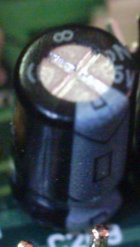
Electrolytic capacitors (see image at left) are polarized, and must be inserted with the negative pin (usually marked with a white stripe, and a negative symbol) closest to the 'stripe' on the component overlay. Special Capacitor notes
The image at right shows two extra 100 nF capacitors (C104 & C105) that must be added to the bottom of the PCB. They both solder to the centre pad under the TO220 FET on the other side. There are two type of 100 nF capacitors (marked as 104) capacitors. Nine (9) of them are lower profile ones that are used between the IC sockets of a number of ICs. This is done to both save space and provide better filtering. Make sure you don't mix these pars as the larger capacitors don't fit between sides of the IC socket. |
DiodesDiodes are also polarised. Most of the smaller ones are installed vertically on the PCB as shown in the image at right, with the diode's band closest to the PCB circle. The 1N5822 (D1) Schottky Diode & 1.5KE-33A (1N6832 = D2) Transorb are installed horizontally with their band matching the stripe marked on the component overlay. Ensure that they are in the correct position before applying power else damage to the diodes and/or the PCB may result. |

|
|
Install the 16 MHz crystal (X1 beside the 28 pin CPU) making sure the metal can doesn't short onto tracks of the PCB. Install the two inductors, which look like large green resistors, vertically as shown. Inductor L1 is near the 28 pin CPU & L2 is near the 8 pin surface mount chip. |
)
IC sockets & TO-220 Package FETPlace the Q1 FET (MTP3055V) in TO-220 package on the PCB as shown at right. Bend the three legs at 90° where the leads taper from thick to thin. We suggest you can bolt the TO-220 package to the PCB before soldering so the hole in the tab aligns perfectly with the hole in the PCB. Note : no insulating washers nor thermal transfer compound is required, as very little power is dissipated by the switch-mode heater circuit. Note that R017 & R108 are 0.150 ohm and R109 is missing. Normally the three resistors are 0.220 ohm and all three are installed. The two configurations are almost electrically identical. |
|
|
|
|
Header Strips, Shunts & Fuse Holders)
A number of single strip headers (6) are used to carry shunts (jumpers). A further header (Y2) has two rows of three pins. Quick overview for jumper shunt usage when the unit is operational :
There are two fuse holder clips. Insert into the PCB taking note that the end location tabs for the fuse are installed correctly. You should check before soldering by inserting the fuse, but remove before actually soldering. |
|
At the bottom edge of the PCB, install the flat green 10 pin connector (Y5) so it rests squarely and on the top side of the PCB. Note : remove the mating connector with the screw terminals before soldering. At the right end of the PCB snap the RJ45 socket (Y1) into the mounting holes on the PCB, ensure it's sitting flush with the PCB, and solder it in place. The clear bodied 2 pin right angled Molex power connector (Y4) is installed so it sits flush with the PCB (as there is no locating tab for it, make sure it is square before soldering). |
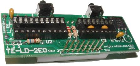
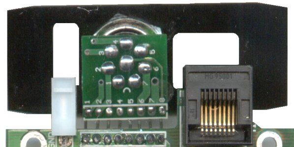
Display PCBThe display PCB is shown at right. There are only minor differences between the (enlarged pop-up) Rev-1 and Rev-2 PCBs. The solder side of the display PCB holds the 3-digit 7-segment display module but it is soldered on the "component side" as shown. |
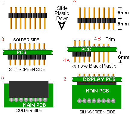
Display Header & PinsCut off a strip of 8 header pins (1. at left). Hold the strip downwards and gently slide down (2.) the black plastic retainer to leave 6 mm above the top of the retainer (and 6 mm below). Solder the header (3.) on the solder side of the display PCB so the black retainer with shorter pins is on the silk screen side. Immediately slide off the black plastic retainer (4A.) while the pins are still hot. Trim the row of pins on the solder side (4B). The pins on the silk-screen side should now be 6.0mm from the surface of the PCB. )
On the main PCB, position the female 8 pin 90° connector on the bottom (5.) of the PCB. Now solder the connector from the silk-screen side. The two PCBs now come together (6). Enlarged image.
|
Lastly, ensure the D2PAK regulator TAB has been soldered correctly, and the two wire links shown in the above images ( Rev-1 & Rev-2) are correctly inserted. Note that the "fixed" display options that must be wired up (or not) are:
Lid, Label and Assembly of LED PCBAlthough this step can be left for later, as it relates to the display, it is presented here. Firstly, cut the mounting post from the case lid, as shown. Leave the other post as this forms a rigid support for the display PCB. Remove the brown paper from the red acrylic window, and install it in the slots in front of the display, with the black painted side on the inside of the case. Place the main PCB with attached LED PCB into the case. Place lid on the case, and close it, noting that the lid has one remaining mounting post to engage the LED PCB ... |
|
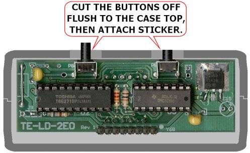
Trim the buttons with very sharp side cutters or use a Dremel so the buttons are almost flush with the case. The green sticky label can be added so it can be read normally when looking at the LED screen. The supplied rubber feet with sticky backing can now be placed at the four corners of the case. |
Extra special attention to mounting the 8 pin circular connector to the end plate using the transition PCB is required. Please read this whole section, and play with the parts mentioned, a few times, before attempting any soldering. A small, but annoying, percentage of wideband problems we fix relate to incorrectly attached 8 pin circular connectors. If after soldering it all together, you thought it was easy, then you probably made a mistake!!!
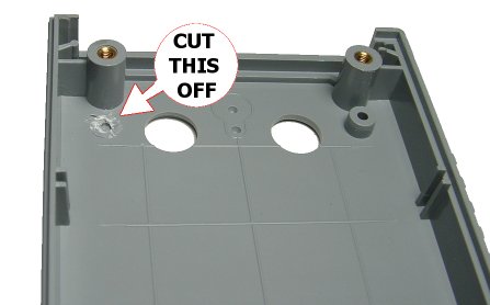
![]() Step 0 - WARNING The case end plate that the circular connector fits in to
may have a flat in the wrong position for connector supplied.
As success relies on everything being aligned properly, you may have to remove the existing flat (with a small round file)
to get everything aligned.
Look at the images below showing this ridge ("location mark/guide") at the bottom of the end plate.
Step 0 - WARNING The case end plate that the circular connector fits in to
may have a flat in the wrong position for connector supplied.
As success relies on everything being aligned properly, you may have to remove the existing flat (with a small round file)
to get everything aligned.
Look at the images below showing this ridge ("location mark/guide") at the bottom of the end plate.
|
Check that connector's internal locating ridge ("location mark/guide" in images below) is positioned at the bottom of the end plate - not necessarily as the flat in the hole would suggest. Note: The hex nut cannot be attached or removed without damage after soldering. This is shown in the image at left, note the spring washer is under the hex nut. After rechecking its orientation, firmly secure the hex nut, but don't twist the housing nor damage the connector's threads. |
|
Step 3 - Solder PCB, with leads, to 8 pin connector lugs. Do not force the PCB onto the lugs of the 8 pin connector. Rather, ease the PCB over the lugs so the lugs are just flush with the PCB face. There should be 1 mm space between the back of the PCB and the metal housing of the connector. Be sure the white semi-circle marked on the PCB matches the locating tab on the other side of the connector (also check that the pins on the PCB now match the small numbers printed on the back of the connector). This is shown in the image at left. Now solder the 8 lugs to the transitions PCB using enough heat to flow solder through the PCB holes and around the lugs. Check that the silkscreen is as shown at left and there's a 1 mm gap between the transition PCB and 8 pin connector. Here's another image of the result. |
|
Step 5 - Adjustment. Vary the bend of the 8 wires, and check that the main PCB will now rest gently into the case without any strain on the main or transitional PCB. Check that the main PCB can be bolted to the case without it flexing. |
Step 6 - Only when you are completely satisfied everything is sitting correctly should you solder the wires to the main PCB. Trim the wire protruding above the PCB. If you make a mistake it will be better to cut the 8 wires and then carefully desolder the resulting 16 solder points, and start again. The image at left and above shows the endplate assembly soldered to the Main PCB. Be aware that any strain on the wires can, in time, cause failure of the connection in high vibration (automotive) environments. Step 7 Check for common faults we regularly see in DIY units that we repair.
|
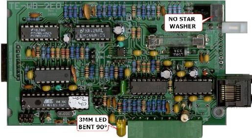
Attaching the PCB to the case.Again, this step can be left until after the electronics testing step. Trim the cutout for the green connector of any loose plastic swarf resulting from the CNC operation on the case. Check that the the 3mm Amber LED has been bent over so it's dome sits flush with the face of the green connector. Place the Wideband assembly into the case, and secure it with a M3x6mm screw and star washer in the mounting hole closest to the RJ45 socket. A M3 6 mm bolt, without star washer, is used to secure the FET's tab. |
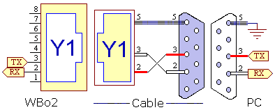
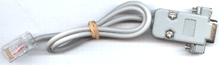
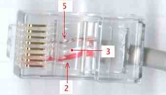
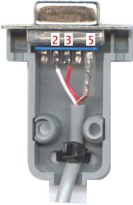
RJ45 to DB9 Serial cableThis shows the construction of the RJ45 to DB9 cable - used for serial comms to PC (or Palm etc.). The RJ45 comes pre-crimped, but check the colours carefully (the locating tab is under the wires in the image). Ensure we have not made a mistake when we crimped the wires into the RJ45 connector. We may have got the pins wrong or we may not have inserted the wires far enough. The RJ45 clear connector is numbered as shown in the image below - the locating tab is under the connector. The DB9 connector may have very small numbers on the outer face that clearly show which pin is which. |
|
At the DB9 end, a cable tie should be used to secure the cable (drill two small holes in the grey backshell). |
|
Note how the cable "crosses over" between pins 2 and 3 between connectors. Now check for end-to-end continuity of the completed cable.
Note that the DB9 connector used is a DB9S or female DB9. It should not have exposed pins, but a DB9 with exposed pins (as found on a PC RS232 port or extension cable) should mate with it. Note also that a one-to-one extension cable should be used to extend the cable (not a null modem cable). |
|
The next thing to do is to rigorously follow the 2E0 test procedure (PDF document, we suggest you print it out). but first read what should be done as preliminary steps to make your testing and debugging more productive ...
One of the biggest problems constructors' seem to have is in building the WBo2 to sensor cable. We see many units where the cable has a short, open, or it's just mis-wired. Take care your cable is robust and correctly made.
Next most common problem is in swapping resistors and/or reversing diodes. You should have checked the value of each resistor before soldering them in, and at the end, check some have not been transposed (it's easy to do when you flip the PCB). Reversed electrolytic capacitors may explode when first powered up, so check carefully.
Visually check the back of the PCB that all components have been soldered. We quite often get DIY kit boards to repair that have parts sitting on the PCB with maybe only one leg soldered in. This can produce a unit that will test OK and run for a time, only to fail when it's most needed. Spend some time to do this carefully and fully. Use a magnifying glass if necessary.
Before applying power, re-read the section above on setting the jumpers. A common problem is testing with an inadequate power supply - the unit needs 12 Volts at up to 3 Amps, but can run at up to about 19 Volts (quite well), and down to just above 10 Volts (but not very well in a real vehicle), so check your supply voltage when it's under load as some supplies may sag when asked to supply the necessary turn-on heater current.
Read the sections that describe what the LEDs do - the 2E0 does not have a small red LED like the other units but the right most decimal point (red status dot) of the display serves this same function. The amber heater LED shows how much power is supplied to the unit - short sharp flashes indicated the firmware is looking for the sensor (unplugged, a bad sensor, or bad sensor cable), or finds the voltage too low to run the sensor (remember, the voltage may sag under load) .
Remember that the sensor must always be installed with its wires pointing upwards by at least 10° to the horizontal (to avoid condensation cracking the sensor). The sensor should be placed where the gas temperature past the sensor is always less than 750°C but we recommend you install where the maximum temperature is closer to 500°C. This often means the sensor is located at least 1 meter (3 feet) or more from the closest exhaust valve, or a similar distance from the turbo outlet. Never place the sensor on the high pressure side of a turbo setup as this is way too hot and the high exhaust back pressure will give you misleading readings (rich shows richer than it is, so you tune too lean under power - not good for long turbo engine life). Remember that the stock narrowband sensor position will almost always be too hot and a good installation will usually require a new bung be welded in, preferably before the catalytic converter.
Placing the sensor at the back of a vehicle in a tail pipe "sniffing" position can cause the sensor to be excessively cooled unless special measures are taken. We suggest you make a special tail pipe adapter where a 20 mm diameter pipe expand out to 30 mm where the sensor is located, and then closes back to 20 mm. The 20 mm sections should be at least 250 mm long. This setup reduces the gas speed past the sensor and gets the sensor tip out of the direct gas flow without affecting the response speed too much.
If you have difficulties then try the Yahoo oz-diy-wb support group but the first question that we'll ask is "have you performed the 2E0 test procedure".
Further information on building WBo2 may be added as problems arise We actively update these pages in response to your feedback.
We appreciate your feedback on the content and any corrections necessary to this article.
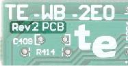 The PCB Rev number is found at the top left of the main board.
Rev 1 and 2 boards differ only slightly (board dimensions changed, some holes enlarged for a better fit and re-arrangement of a couple of parts near the display end of the main PCB).
The PCB Rev number is found at the top left of the main board.
Rev 1 and 2 boards differ only slightly (board dimensions changed, some holes enlarged for a better fit and re-arrangement of a couple of parts near the display end of the main PCB).
)
)
 You may need to wiggle the display PCB slightly to get the case to close
as it has a tendency to move inwards and not engage the slot between the two remaining posts.
Note: NO brute force is necessary.
You may need to wiggle the display PCB slightly to get the case to close
as it has a tendency to move inwards and not engage the slot between the two remaining posts.
Note: NO brute force is necessary.
)
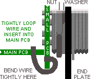 Step 4 - Bend the wire tightly around under the small PCB, and into a loop, as shown in the images.
Insert the 8 leads into the main PCB's holes from underneath.
Step 4 - Bend the wire tightly around under the small PCB, and into a loop, as shown in the images.
Insert the 8 leads into the main PCB's holes from underneath.
)
)
)
)
)
)
)