|
|

The 2A1 DIY kit is a variant of the 2A0 DIY kit. The difference being 2A0's 32 kbyte of on-board logging memory has been replaced by a 1 M byte module. The 32 kbyte memory is implemented as a single 8 pin DIP chip (U2) and some resistors, whereas the 1 Mbyte memory is a pre-built SMD PCB module that plugs into a 12 pin PCB header (Y5).
|
Tech Edge once sold the 2A0 and 2A1as pre-built units. Since December 2006 the 2A0 and 2A1 have been available only as DIY kits, and the newer 3A series are only available as pre-built units. Go here for the 2A1 User Guide page which describes the 2A1's capabilities. |
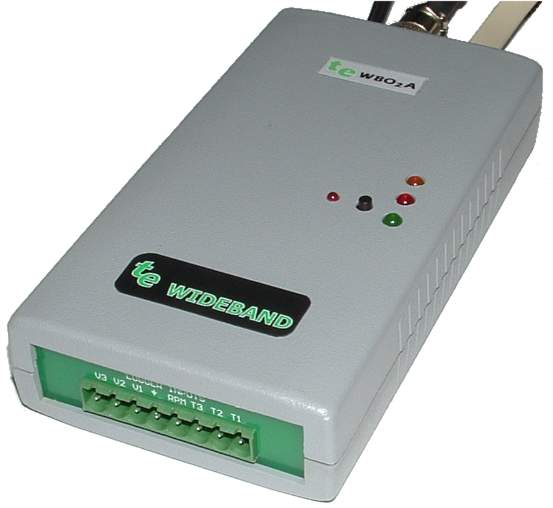
To build the 2A1 you start by reading the section below, but essentially you are building the 2A0 with some modifications. The same 2A0 test procedure is also used. This pictorial link shows images of the 2A0 to 2A1 conversion but is useful to show the area where parts are left off, or where parts are placed under the PCB.
| Here is a PDF document showing the parts location and parts value overlays as well as a parts list. The two images are also available as links below. |
Start by carefully noting the special areas of the overlay where parts are left off - these parts are shown in bright blue in the 2A1 parts locations overlay. There are some parts in bright red that are installed under the PCB (on the solder side).
The 2A1 component values overlay is probably more important, and shows the same points noted in the previous paragraph (but uses different colours). Here is a list of changes from the 2A0 build:
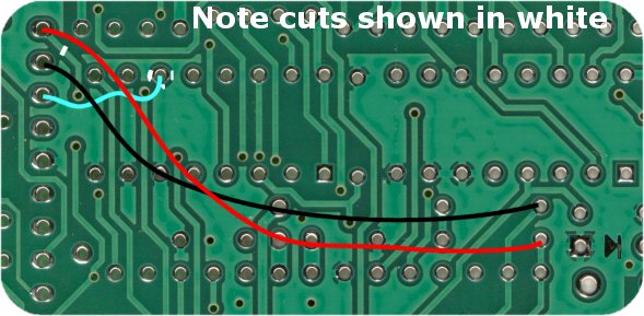
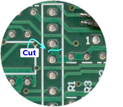
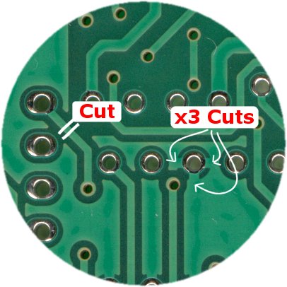
Having noted the above changes, and before you install any parts, start by cutting some tracks on the PCB. The circular images can be enlarged by clicking on them. To further aid location of the areas to be cut, the small rectangular images can be clicked to help you locate the exact area on the PCB referred to. These locations images are also here - component side, and the solder side, as well as wires added later.
|
|
