(22 October '04) -- These notes should help you construct your own TE WBo2 (2A0)
Bosch LSU4 / NTK L1H1 oxygen sensor interface unit.
As noted in the location guide,
there is a rev-2, rev-3 and now Rev-4 PCB with only small
differences you need to be aware of.
For the rev-4 PCB, the major change is removal of some jumpers,
and the addition of the NTK jumper, which should be ON for the LSU version and OFF
for the NTK version (yes, it should be called the LSU jumper).
For the rev-3 PCB the NTK version has a small resistor difference that is noted below.
Please read all text before you start
as many procedures should be perform in sequence.
Many of the images below can be enlarged by clicking on them.
Firstly inspect your bare PCB for any shorts between adjacent tracks.
We normally have very few problems of this nature, but we'll sometimes
get a batch of PCBs (from a single panel) that have been under-etched,
resulting in an odd hairline short.
It's best to find any board faults before you've built the unit
because the IC sockets often make it difficult to find shorts afterwards.
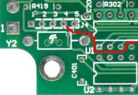
Modifications Required to the rev-2 PCB
You should find one trace that has been removed (on the 2A0 rev-2 PCB, not the rev-3 PCB), this is shown in
the image at left as the RED trace.
Note also that the PCB comes with the DAC7612 device already soldered in
as some may find the SOIC-8 (8 pin) difficult to mount correctly.
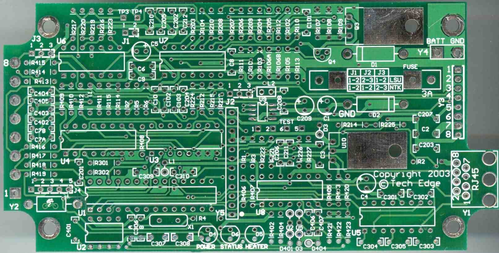
If you haven't already done so, you should go here and
print off component location image(s).
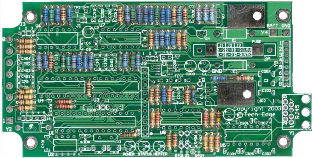
Getting Started
The silkscreen has visual cues for using 1% or 5% resistors.
The 1% resistors having a dotted line as shown in the blowup at right.
5% Resistors are also marked in Yellow on the
Color Component Overlay, While 1% Resistors are marked as Green
It is important that 5% resistors are not used where a 1% resistors is called for.
But it's okay to use a 1% in place of a 5%.
We may actually substitute a 5% with 1% in the parts kit from time to time,
but we will never substitute a 1% with a 5%.
Note 1 : all the 100 ohm resistor can be substituted with
5% resistors without loss of accuracy - the overlay shows these as 1% items on the rev-2 and rev-3 PCB.
Note 2 : Resistors, in the kits, are marked in text without the k.
Thus, 20 means 20 k.
But, resistors less than 1 k are marked with an R, so 910 ohms is marked as 910 R.
However, measure all resistors before using them to check we have not made a mistake,
or you have not misunderstood our marking scheme.
5% Resistors
First we insert the physically lowest components - these are the resistors, and
we have inserted just the 5% resistors first as these are more numerous.
The 5% resistors will all have just 4 coloured bands with an extra gold band indicating
the 5% tolerance.
5% resistors typically have a beige or light brown background.
It's best to orient them with the gold band to the right and to the top so
the values can be most easily read from left to right and bottom to top as
the silkscreen is printed.
1% Resistors (see notes 1 & 2)
Next the 1% resistors go in.
Note that the three 0.22 ohms resistors (top mid right, very light blue) may be supplied
as either 2% with a red band rather than brown (most likely),
or in some instances, as a 5% (with standard gold band).
Note 1 :R214 is 82 k for the NTK version but 910 ohms for the LSU version.
It is very important that the correct resistor is used, particularly for the NTK version as the
sensor can be damaged if the 910 ohm resistor is used. Note also that the NTK or LSU versions
requires the correct firmware version for correct operation.
Lastly, (as noted below too) the header shunts should now always be placed in the LSU position.
Note 2 : Despite the images and silkscreen showing all the 100 ohms resistors as being 1%,
there are only two (R204, R205) that should be 1%, and even then there's no problem using 5%,
so don't worry if all 100 ohms are 5% (or if they are all 1%).
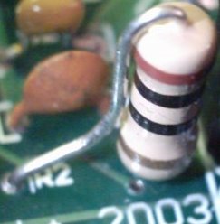
The image shows resistor R2 (10 Ohms 1 Watt) mounted vertically as it will not fit easily horizontally.
In practice, it may be easier to put R2 in as one of the last operations
as this will aid assembling more of the components that sit low to the PCB.
Note : R401 (= 15k 1W) is the large resistor outline in the lower
left corner (marked with "cyclist" symbol on Rev-2 PCBs).
At this stage we should have all the 1% and 5% 1/4 watt resistors in place.
We can now put in the capacitors and diodes as described below.
Capacitors
Capacitors come in a few different forms, and it is important to use the correct ones.
Typically block monolithic, ceramic, and polyester capacitors
are not polarized, This means you may insert them either way around.
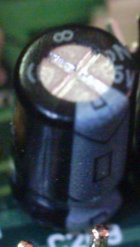
Electrolytic capacitors (see image at left) are polarized, and must be inserted with the
negative pin (usually marked with a white stripe, and a negative symbol)
closest to the 'stripe' on the component overlay.
The image at right (rev-2 PCB) shows two extra 100 nF (104) capacitors (SNUB1 & SNUB2)
that must be added to the bottom of the PCB. They both solder to the centre TO220 pad.
The rev-3 PCB has holes for these capacitors but they are still located under the PCB.
Note that (for the rev-2 PCB) C212, C7B & C306B are not installed on the PCB.
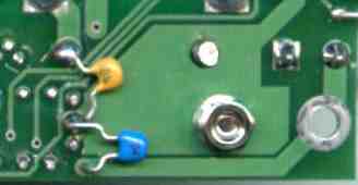
Diodes
Diodes are also polarised. Most are installed vertically on the PCB as
shown in the image at right, with the diode's band closest to the PCB circle.
Make sure you install the 1N4746A zener diode (D403, shown as "03" on the overlay) in the
correct position as it is easily confused with the 1N4148 (slightly smaller) diodes alongside.
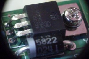
The 1N5822 (D1) Schottky Diode & 1N6832 1.5KE-33A (D2) Tranzorb are installed horizontally
with their band matching the stripe marked on the component overlay.
Ensure that they are in the correct position before applying power else
damage to the diodes and/or the PCB may result.
Install the 16 MHz Crystal (X1).
It may help to install the 28 pin socket at the same time as they will then both be a better fit.
Install the 2 Inductors (L1) & (L2) vertically as shown.
IC sockets & TO-220 Packages
Place the TO-220 (7805 and MTP3055V) packages into the PCB from the top, and bend their legs
over 90 degrees so they lay flat on the PCB. Bolt the TO-220's to the PCB using the supplied
M3 screws, star washers, and nuts, and lastly solder them into the PCB.
Note : no insulator washers or thermal transfer compound is required, as very little
power is dissipated by the switchmode heater circuit and low current 5 Volt supply.
LEDs and IC Sockets
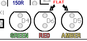
Now the LEDs are installed (although it has been suggested this should be the last step before switching on).
The image shows the position of each coloured LED and also the flat at the
base of each LED which must be oriented away from PCB's edge.
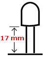
Note that the bottom surface of each LED should be 17 mm from the surface of the PCB (see the next image at left)
so they just protrude through the pre-drilled holes in the case's lid.
One way to get the LED clearance just right is to use a piece of soft, but rigid card (height = 17 mm)
as a temporary spacer under the LED while it is soldered.
The LED's legs may need to be bent a little so they align with the pre-drilled holes in the case.
If you made the legs a little longer, then they can be reduced in height by kinking the legs a little,
rather than the more drastic resoldering.
Lastly, put in the IC sockets noting that their pin 1 indent is correct (to the left or top).
Y5 header pins (2 & 3 is the rescue re-flash option) should not have any shunts on them.
NTK jumper should be installed for the LSU (yes, it's reversed logic!)
Note 1 (Rev-4 PCB) :
Make sure you read Changes/Modifications section in the Location Guide
that relate to the removal of J2 from the rev-4 PCB.
Rev-4 also requires the new NTK terminal block (it will be a tight fit in the PCB).
Note 2 (Rev-3 PCB) : if you are constructing the NTK version then you should
still put the jumpers in the LSU position - in fact, we now recommend that you don't use a header,
but simply put in wire links (cut from the ends of resistors leads).
For Rev-2 PCBs, cut the supplied 13 pin 0.1" header strip into
a 5 pin (J4), 3 pin x two (J2, J3), & a 2 pin (J1) length.
Each short header strip will require a shunt that can be placed there after soldering.
For Rev-3 PCBs, cut three 3 pin (J2, J3, J4), & a 2 pin (J1) length.
You will be left with two pins that can be soldered into the Y5 2-3 position (force re-flash function).
For Rev-4 PCBs, cut a 3 pin (J4), & a 2 pin (J1) length (solder a link for J3).
You will be left with 8 pins that can be soldered into the Y5 1-8 position.
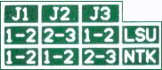
As noted above, the image at left, taken from the PCB area under the fuse, was intended
to show how the jumper block or shunts, should be placed
on the header strips. However, the design was changed and the LSU only position should now be used.
J4 should be in the 1-2 position for 12 Volt (or COIL) operation,
but for lower voltage (RPM from ECU) operation J4 is in the 2-3 (rev-3 and up PCB) or 4-5 position (rev-2 PCB only) .
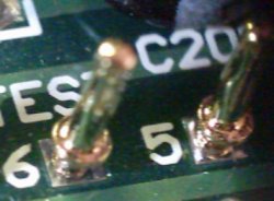
Insert the 6 gold test point pins into the PCB at the points marked as
TEST 1, 2, 6, 5 (near centre of PCB) & TP3, TP4 (top left).
Note, the pins have a shorter thick end and a longer thin end.
The thin end should be inserted into the PCB from the top (it may still be a tight fit -
do not force the pin, check you have the right end).
Solder and then cut off the long protruding pin on the solder side of the board.
For the two fuse holder clips, insert into the PCB and solder,
taking note the little tab that locates the fuse are installed to the outer sides.
You should check before soldering by inserting the fuse, but remove before soldering though.
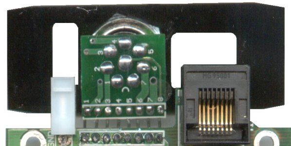
Logger Connector, RJ45 & Power Connector
At the left of the PCB, install the flat green 8 pin connector (Y2 for the logger)
so it rests on the top side of the PCB.
Note : remove the mating connector with the screw terminals before soldering.
At the other end of the PCB,
snap the RJ45 socket Y1 into the mounting holes on the PCB,
ensure it's sitting flush with the PCB, and solder it in place.
The clear bodied 2 pin right angled Molex power connector
is installed in Y4 so it sits flush with the PCB (as there is no locating tab for it, make sure it is
square before soldering).
8 pin Circular Sensor Connector & Transition PCB
Step 1 - Special attention to the mounting of the 8 pin circular connector is required.
The connector must FIRST be attached to the black endplate,
using the large hex nut and spring washer.
Note the end plate has a locating flat for the connector.
You must secure the connector before the small PCB is soldered to the 8 pin connector.
The hex nut cannot be attached or removed without damage afterwards.
This is shown in the image at left, note the spring washer is under the hex nut.
Firmly secure the hex nut, but don't twist the housing nor damage the connector's threads.
Step 2 - Prepare the transition PCB with leads.
Cut spare wire from resistor legs etc. into 1" (25 mm) lengths.
Solder these to the small PCB so they protrude from the solder side (ie. solder on the silkscreen overlay side).
The image at right shows this.
Step 3 - Solder PCB, with leads, to 8 pin connector lugs.
Do not force the PCB onto the lugs of the 8 pin connector.
Rather, ease the PCB over the lugs so the lugs are just flush with the PCB face.
There should be space between the back of the PCB and the metal housing of the connector.
Be sure the white semi-circle marked on the PCB
matches the locating tab on the other side of the connector
(also check that the pins on the PCB now match the small numbers printed on the back of the connector).
This is shown in the image at left.
Step 4 - Bend the wire around under the small PCB, and into a tight loop.
Insert the 8 leads into the main PCB's holes from underneath.
Don't solder yet!
The endplate assembly, should now "fold up" into the
correct position, with the RJ45 poking out through the large square hole,
and the power connector visible through the slot.
Step 5 - Adjustment and soldering.
Vary the bend of the 8 wires, and check that the main PCB will now rest gently
into the grey case without any strain on the main or transitional PCB.
Check that the main PCB can be bolted to the case without it flexing.
Only when you are completely satisfied everything is sitting correctly should you solder the wires to the main PCB.
If you make a mistake it will be better to cut the 8 wires and then carefully desolder the resulting 16
solder points, and start again.
The image shows how to connect the endplate assembly to the Main PCB.
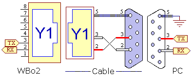
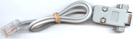
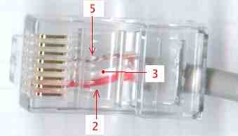
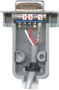
RJ45 to DB9 Serial cable
This shows the construction of the RJ45 to DB9 cable - used for serial comms to PC (or Palm etc.).
The RJ45 comes pre-crimped, but check the colours carefully (the locating tab is under the wires in the image).
At the DB9 end, a cable tie should be used to secure the cable (drill two small holes in the grey backshell).
Note how the cable "crosses over" between pins 2 and 3 between connectors.
Re-checking and Next Steps(s)
One of the biggest problems constructors' seem to have is in building the WBo2 to sensor cable.
We see many units where the cable has a short, open, or it's just miswired. Take care your cable is robust and correctly made.
Next most common problem is in swapping resistors and/or reversing diodes (and even the TO-220 FET and TO-220 5V regulator).
You should have checked the value of each resistor before soldering them in,
and at the end, check some have not been transposed (it's easy to do when you flip the PCB).
Reversed electrolytic capacitors may explode with power, so check carefully.
Before powering up, re-read the section on setting the jumpers.
A common problem is testing with an inadequate power supply - the unit needs 12 Volts at up to 3 Amps,
but can run at up to about 19 Volts, and down to just above 10 Volts, so check your supply voltage when
it's under load as some supplies may "sag" when asked to supply the necessary turn-on heater current.
Read the sections that describe what the LEDs do - the green LED should always be on, and the red LED
should flash for the first 20 seconds of so until the heater get up to temperature. The amber LED
shows how much power is supplied to the unit - short sharp flashes indicated the firmware is looking
for the sensor, or finds the voltage too low to run the sensor.
A batch of Rev-3 PCBs did have some "micro shorts", but all PCBs are now 100% tested (so we expect about 99.5% PCB success rate!)
RPM Input Changes
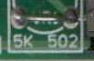
An optional preset pot (5 k ohm) was added to the RPM input circuitry (this will normally not be required)
- this component is found in the lower left of the PCB and a wire link should be added from the 5K
point to the 502 point. The image shows this link.
On-Board Logging Changes
To support on-board logging a number of changes were made -
refer the Logging Hardware page for more information.
Further information
Further information on building WBo2 may be added as problems arise (01 Nov. '04).
We actively update these pages in response to your feedback.
We appreciate your feedback on the content and any corrections necessary to this article.


 RPM Input Changes