![]() | 2A0 Main
| 2A0 DIY
| 2A1 Main
| 2A1 DIY
| Logging Info
| 1 Mbyte hardware
| 32 kByte hardware
| 2A0 Main
| 2A0 DIY
| 2A1 Main
| 2A1 DIY
| Logging Info
| 1 Mbyte hardware
| 32 kByte hardware
)
)
This page describes the 1 MegaByte logger upgrade that has been available for all 2A0 pre-built units and DIY kits since late August 2005. It increases 2A0's on-board logging capacity by 32 times. Logging times to tens of minutes, at the fastest logging rate, are now possible. 2A0 units with this addition are known as the 2A1. Brief History : 2A0 was originally released with no on-board logging memory, but it had provision for up to 32 kBytes. With the Rev-3 2A0 PCB, the optional 32 k on-board logging memory was made standard and supplied with both DIY and pre-built units. Memory upgrade : involves modifications to existing 2A0 units, including removal of the current 32 kbyte TWI EE memory for 1 Mbyte SPI EE memory. A processor upgrade is also made to cater for the increased code needed to drive the extra memory. All 2A0 units can be modified and the parts to do this are available as a DIY upgrade kit. Electronic construction skills are involved in making the upgrade but should be easy if you built your own 2A0 unit. Tech Edge can make the changes for you if you purchased a pre-built unit. |
Logging is controlled by a single switch on the top of the 2A0 case. User feedback for on-board logging is provided by WBo2's red LED (which also provides general-status feedback). More information on how logging works can be found on the detailed WBo2 Logging Information page.
If you're going to make the changes yourself then here's how it's done. Remember that Tech Edge can make the changes for you, for a small fee, if you prefer. We may be able to advise of people in your local area who can also do this. All red links below are to pop-up images, but you need JavaScript enabled for this feature. Alternatively, go here for all the images in one place.
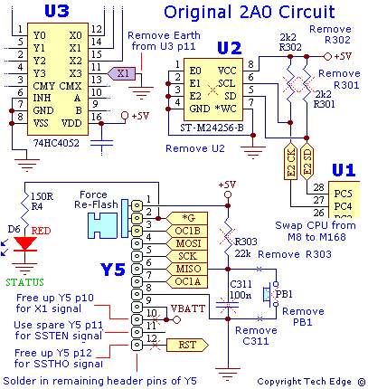
The original 2A0 on-board logging circuit, with 32 kbyte EE memory using TWI (Two Wire Interface, but also know as the Philips I2C bus), is shown at far right. Full schematics are available here so we have just shown the important sections and changes required. Basically the processor's TWI control pins (27 & 28) are now used to control an SPI interfaced chip, and an unused MUX input X1 is used to sense the new logger control-button. The processor SPI signals MOSI, MISO & SCK are already available on the Y5 connector, but two Y5 pins (10 & 12) must be freed up for the old TWI signals. Note that Y5 pin 11 was originally unassigned and is available for use. Here's what you have to do :
)
)
At left is the schematic of the modified 2A0. Click on the image to see the logger module's schematic. )
One major task remains, drilling the holes for the module's press-button and 3 mm LED. This is made easier as the case has an accurate grid that can be used to mark the hole centres. Take care to do this as a miscalculation here can make a mess of the case. We recommend you use a drill press for best accuracy, and feed the drill very slowly. The ABS plastic tends to grab when using a general purpose drill bit so make sure you firmly hold down the case, and drill from inside (the side shown).
Hole dimensions are shown at right (enlarge).
Note that both new holes have centres 2 mm to the right of the indicated grid line.
As a reminder of the finihed product's appearance, click on the image at left to enlarge. You may find that the hole you drilled for the button may need some filing or enlarging to get the button to operate freely. Make sure you check the fit of the holes etc. with the main PCB screwed down as the PCM can move around a little under the 4 screws. |
Kit Parts & Module Details)
)
At left is what you get in the 2A0->2A1 upgrade kit. Click to enlarge x2. The actual parts list is described in the next section. The purpose of the label is to cover up the hole that would be left when the logger button is relocated. At right is the layout of the logger module itself. Not shown is the logger button, and the 3 mm red LED. To see an enlarged version of the module click here or the image. Or for the module's schematic, |
| 1 | 2A-1ML | pre-built & tested 1 Mbyte logger module for 2A0 ("Megabyte Logger") |
| 1 | Y5 | 12 pin header (maybe 3 spare pins for some installations) |
| 1 | U1 | Mega-168 preprogrammed processor |
| 1 | R1 | 1k5 5% resistor - replaces original R1 possibly damaged |
| 1 | R406 | 47k 5% resistor - replaces original R406 possibly damaged |
| 1 | red wire | 55 mm long "wire wrap" wire |
| 1 | black wire | 55 mm long "wire wrap" wire |
| 1 | blue wire | 15 mm long "wire wrap" wire |
| 1 | label | te Wideband label covers existing logger button hole |
)
)
)
)
)
)